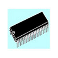
ST72T774J9B1 STMicroelectronics, ST72T774J9B1 Datasheet - Page 114

ST72T774J9B1
Manufacturer Part Number
ST72T774J9B1
Description
Manufacturer
STMicroelectronics
Datasheet
1.ST72T774J9B1.pdf
(144 pages)
Specifications of ST72T774J9B1
Cpu Family
ST7
Device Core Size
8b
Frequency (max)
24MHz
Interface Type
I2C/USB
Program Memory Type
EPROM
Program Memory Size
60KB
Total Internal Ram Size
1KB
# I/os (max)
31
Number Of Timers - General Purpose
1
Operating Supply Voltage (typ)
5V
Operating Supply Voltage (max)
5.5V
Operating Supply Voltage (min)
4V
On-chip Adc
1-chx8-bit
On-chip Dac
1-chx8-bit
Instruction Set Architecture
CISC
Operating Temp Range
0C to 70C
Operating Temperature Classification
Commercial
Mounting
Through Hole
Pin Count
42
Package Type
SPDIP
Lead Free Status / Rohs Status
Specific Sites Compliant
Available stocks
Company
Part Number
Manufacturer
Quantity
Price
Part Number:
ST72T774J9B1
Manufacturer:
ST
Quantity:
20 000
ST72774/ST727754/ST72734
DDC INTERFACE (Cont’d)
DDC1/2B CONTROL REGISTER (DCR)
Read / Write
Reset Value: 0000 0000 (00h)
Bit 7 = Reserved.
Forced by hardware to 0.
Bit 5 = EDF End of Download interrupt Flag .
This bit is set by hardware and cleared by
software.
Bit 4 = EDE End of Download interrupt Enable .
This bit is set and cleared by software.
Bits 6, 3:2 = CF[2:0] Configuration bits.
These bits are set and cleared by software only
when the peripheral is disabled (HWPE = 0). They
define which EDID structure version is used and
which Device Addresses are recognized as shown
in the following table:
114/144
0: Download not started or not completed yet.
1: Download completed. Last byte of data struc-
0: Interrupt disabled.
1: A DDC1/2B interrupt is generated if EDF bit is
7
0
CF[2:0] Bit
Values
ture (relative address 7Fh or FFh) has been
stored in RAM.
set.
000
001
010
011
100
101
110
111
CF2
EDF
EDID version used
EDE
v2 + P&D
v2 + P&D
DDC v2
DDC v2
FPDI-2
P&D
CF1
CF0
DDC1 Mode support / Transition Mode support
WP
HWPE
0
Yes (128b EDID) / Yes
Yes (128b EDID) / Yes
Reserved
Reserved
Bit 1 = WP Write Protect .
This bit is set and cleared by software.
Bit 0= HWPE Peripheral Enable .
This bit is set and cleared by software.
ADDRESS POINTER HIGH REGISTER (AHR)
Read / Write
Reset Value: see Register Map
AHR contains the 8 MSB’s of the 16-bit address
pointer. It therefore defines the location of the 256-
byte block containing the data structure within the
CPU address space.
Note: AHR0 is ignored when CF[1:0] = 10 (P&D+ v2
MSB
No
No
No
No
0: Enable writes to the RAM.
1: Disable DMA write transfers and protect the
0: Release the SDA port pin and ignore Vsync
1: Enable the DDC Interface and respond to the
7
RAM content. CPU writes to the RAM are not
affected.
and SCL port pins. The other bits of the DCR
and the content of the AHR are left un-
changed.
DDC1/DDC2B protocol.
mode) to allow non-overlapping 128-byte and 256-
byte data structures.
d sd
d sd
DDC2B Addresses Recognized
@ A2h/A3h
@ A2h/A3h
@ A6h/A7h
@ A2h/A3h
128b-EDID
@A0h/A1h
256b-EDID
128b-EDID
@A0h/A1h
256b-EDID
256b-EDID
128b-EDID
@A0h/A1h
128b-EDID
@A0h/A1h
256b-EDID
LSB
0


