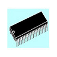
ST72T774J9B1 STMicroelectronics, ST72T774J9B1 Datasheet - Page 28

ST72T774J9B1
Manufacturer Part Number
ST72T774J9B1
Description
Manufacturer
STMicroelectronics
Datasheet
1.ST72T774J9B1.pdf
(144 pages)
Specifications of ST72T774J9B1
Cpu Family
ST7
Device Core Size
8b
Frequency (max)
24MHz
Interface Type
I2C/USB
Program Memory Type
EPROM
Program Memory Size
60KB
Total Internal Ram Size
1KB
# I/os (max)
31
Number Of Timers - General Purpose
1
Operating Supply Voltage (typ)
5V
Operating Supply Voltage (max)
5.5V
Operating Supply Voltage (min)
4V
On-chip Adc
1-chx8-bit
On-chip Dac
1-chx8-bit
Instruction Set Architecture
CISC
Operating Temp Range
0C to 70C
Operating Temperature Classification
Commercial
Mounting
Through Hole
Pin Count
42
Package Type
SPDIP
Lead Free Status / Rohs Status
Specific Sites Compliant
Available stocks
Company
Part Number
Manufacturer
Quantity
Price
Part Number:
ST72T774J9B1
Manufacturer:
ST
Quantity:
20 000
ST72774/ST727754/ST72734
I/O PORTS (Cont’d)
Table 7. I/O Pin Functions
4.1.2 Common Functional Description
Each port pin of the I/O Ports can be individually
configured under software control as either input
or output.
Each bit of a Data Direction Register (DDR)
corresponds to an I/O pin of the associated port.
This corresponding bit must be set to configure its
associated pin as output and must be cleared to
configure its associated pin as input (Table 7, “. I/O
Pin Functions,” on page 28). The Data Direction
Registers can be read and written.
The typical I/O circuit is shown on
write to an I/O port updates the port data register
even if it is configured as input. Any read of an I/O
port returns either the data latched in the port data
register (pins configured as output) or the value of
the I/O pins (pins configured as input).
Remark: when an I/O pin does not exist inside an
I/O port, the returned value is a logic one (pin
configured as input).
At reset, all DDR registers are cleared, which
configures all port’s I/Os as inputs with or without
pull-ups (see
Register
initialized at reset.
4.1.2.1 Input mode
When DDR=0, the corresponding I/O is configured
in Input mode.
In this case, the output buffer is switched off, the
state of the I/O is readable through the Data
Register address, but the I/O state comes directly
28/144
Map). The Data Registers (DR) are also
DDR
0
1
Table 8
to
Table 12 I/O Ports
MODE
Output
Input
Figure
15. Any
from the CMOS Schmitt Trigger output and not
from the Data Register output.
4.1.2.2 Output mode
When DDR=1, the corresponding I/O is configured
in Output mode.
In this case, the output buffer is activated
according to the Data Register’s content.
A read operation is directly performed from the
Data Register output.
4.1.2.3 Analog input
Each I/O can be used as analog input by adding an
analog switch driven by the ADC.
The I/O must be configured in Input before using it
as analog input.
The CMOS Schmitt trigger is OFF and the analog
value directly input through an analog switch to the
Analog to Digital Converter, when the analog
channel is selected by the ADC.
4.1.2.4 Alternate mode
A signal coming from a on-chip peripheral can be
output on the I/O.
In this case, the I/O is automatically configured in
output mode.
This must be controlled directly by the peripheral
with a signal coming from the peripheral which
enables the alternate signal to be output.
A signal coming from an I/O can be input in a on-
chip peripheral.
Before using an I/O as Alternate Input, it must be
configured in Input mode (DDR=0). So both
Alternate Input configuration and I/O Input
configuration are the same (with or without pull-
up). The signal to be input in the peripheral is taken
after the CMOS Schmitt trigger or TTL Schmitt
trigger for SYNC.
The I/O state is readable as in Input mode by
addressing the corresponding I/O Data Register.


