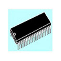
ST72T774J9B1 STMicroelectronics, ST72T774J9B1 Datasheet - Page 89

ST72T774J9B1
Manufacturer Part Number
ST72T774J9B1
Description
Manufacturer
STMicroelectronics
Datasheet
1.ST72T774J9B1.pdf
(144 pages)
Specifications of ST72T774J9B1
Cpu Family
ST7
Device Core Size
8b
Frequency (max)
24MHz
Interface Type
I2C/USB
Program Memory Type
EPROM
Program Memory Size
60KB
Total Internal Ram Size
1KB
# I/os (max)
31
Number Of Timers - General Purpose
1
Operating Supply Voltage (typ)
5V
Operating Supply Voltage (max)
5.5V
Operating Supply Voltage (min)
4V
On-chip Adc
1-chx8-bit
On-chip Dac
1-chx8-bit
Instruction Set Architecture
CISC
Operating Temp Range
0C to 70C
Operating Temperature Classification
Commercial
Mounting
Through Hole
Pin Count
42
Package Type
SPDIP
Lead Free Status / Rohs Status
Specific Sites Compliant
Available stocks
Company
Part Number
Manufacturer
Quantity
Price
Part Number:
ST72T774J9B1
Manufacturer:
ST
Quantity:
20 000
I²C SINGLE MASTER BUS INTERFACE (Cont’d)
4.7.4 Functional Description (Master Mode)
Refer to the CR, SR1 and SR2 registers in
4.7.5. for the bit definitions.
By default the I
(M/IDL bit is cleared) except when it initiates a
transmit or receive sequence.
To switch from default idle mode to Master mode a
Start condition generation is needed.
Start condition and Transmit Slave address
Setting the START bit causes the interface to
switch to Master mode (M/IDL bit set) and
generates a Start condition.
Once the Start condition is sent:
– The EVF and SB bits are set by hardware with
Then the master waits for a read of the SR1
register followed by a write in the DR register with
the Slave address byte, holding the SCL line low
(see
Then the slave address byte is sent to the SDA line
via the internal shift register.
After completion of this transfer (and acknowledge
from the slave if the ACK bit is set):
– The EVF bit is set by hardware with interrupt
Then the master waits for a read of the SR1
register followed by a write in the CR register (for
example set PE bit), holding the SCL line low
(see
Next
Transmitter mode.
Master Receiver
Following the address transmission and after SR1
and CR registers have been accessed, the master
receives bytes from the SDA line into the DR
register via the internal shift register. After each
byte the interface generates in sequence:
an interrupt if the ITE bit is set.
generation if the ITE bit is set.
Figure 54
Figure 54
the
master
2
Transfer sequencing EV1).
Transfer sequencing EV2).
C interface operates in idle mode
must
enter
Receiver
Section
or
– Acknowledge pulse if if the ACK bit is set
– EVF and BTF bits are set by hardware with an in-
Then the interface waits for a read of the SR1
register followed by a read of the DR register,
holding the SCL line low (see
sequencing EV3).
To close the communication: before reading the
last byte from the DR register, set the STOP bit to
generate the Stop condition. The interface goes
automatically back to idle mode (M/IDL bit
cleared).
Note: In order to generate the non-acknowledge pulse af-
Master Transmitter
Following the address transmission and after SR1
register has been read, the master sends bytes
from the DR register to the SDA line via the internal
shift register.
The master waits for a read of the SR1 register
followed by a write in the DR register, holding the
SCL line low (see
EV4).
When the acknowledge bit is received, the
interface sets:
– EVF and BTF bits with an interrupt if the ITE bit
To close the communication: after writing the last
byte to the DR register, set the STOP bit to
generate the Stop condition. The interface goes
automatically back to idle mode (M/IDL bit
cleared).
Error Case
– AF: Detection of a non-acknowledge bit. In this
Note: The SCL line is not held low.
terrupt if the ITE bit is set.
is set.
case, the EVF and AF bits are set by hardware
with an interrupt if the ITE bit is set. To resume,
set the START or STOP bit.
ter the last received data byte, the ACK bit must be
cleared just before reading the second last data
byte.
ST72774/ST727754/ST72734
Figure 54
Transfer sequencing
Figure 54
Transfer
89/144


