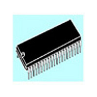
ST72T774J9B1 STMicroelectronics, ST72T774J9B1 Datasheet - Page 99

ST72T774J9B1
Manufacturer Part Number
ST72T774J9B1
Description
Manufacturer
STMicroelectronics
Datasheet
1.ST72T774J9B1.pdf
(144 pages)
Specifications of ST72T774J9B1
Cpu Family
ST7
Device Core Size
8b
Frequency (max)
24MHz
Interface Type
I2C/USB
Program Memory Type
EPROM
Program Memory Size
60KB
Total Internal Ram Size
1KB
# I/os (max)
31
Number Of Timers - General Purpose
1
Operating Supply Voltage (typ)
5V
Operating Supply Voltage (max)
5.5V
Operating Supply Voltage (min)
4V
On-chip Adc
1-chx8-bit
On-chip Dac
1-chx8-bit
Instruction Set Architecture
CISC
Operating Temp Range
0C to 70C
Operating Temperature Classification
Commercial
Mounting
Through Hole
Pin Count
42
Package Type
SPDIP
Lead Free Status / Rohs Status
Specific Sites Compliant
Available stocks
Company
Part Number
Manufacturer
Quantity
Price
Part Number:
ST72T774J9B1
Manufacturer:
ST
Quantity:
20 000
DDC INTERFACE (Cont’d)
4.8.5 DDC Standard
The DDC standard is divided in several data
transfer protocols: DDC1, DDC2B, DDC/CI.
For DDC1/2B, refer to the “VESA DDC Standard
v3.0” specification. For DDC/CI refer to the “VESA
DDC Commands Interface v1.0”
– DDC1 is a uni-directional transmission of EDID
– DDC2B is a uni-directional channel from display
– DDC/CI is a bi-directional channel between the
Note: The DDC2AB standard is no longer handled by the
4.8.5.1 DDC1/2B Interface
4.8.5.1.1 Functionnal description
Refer to the DCR, AHR registers in
for the bit definitions.
The DDC1/2B Interface acts as an I/O interface
between a DDC bus and the microcontroller
memory. In addition to receiving and transmitting
serial data, this interface directly transfers parallel
data to and from memory using a DMA engine,
only halting CPU activity for two clock cycles
during each byte transfer.
The interface supports by hardware:
– Two DDC communication protocols called DDC1
Table 25. Valid Device Addresses and EDID structure
Device Address
EDID v1:
A0h / A1h = 1010 000x
EDID v2:
A2h / A3h = 1010 001x
EDID v2:
A6h / A7h = 1010 011x
reserved
v1 (128 bytes) from display to host clocked by
VSYNCI.
to host. The host computer uses base-level I
commands to read the EDID data from the dis-
play which is always in slave mode.
Specific types of display contain EDID at fixed
I
Table
host computer and the display. The DDC/CI of-
fers a display control interface based on I
It includes the DDC2Bi and DDC2AB standards.
and DDC2B.
2
C device addresses within the device (refer to
interface.
25).
CF2 bit
Section
0
0
1
1
1
x
2
C bus.
4.8.6.
CF1 bit
2
C
x
0
1
1
1
x
– Write operations into RAM.
– Read operations from RAM.
In DDC1, the interface reads sequential EDID v1
data bytes from the microcontroller memory, and
transmits them on SDA synchronized with Vsync.
In DDC2B mode, it operates in I
The DDC1/2B Interface supports several DDC
versions configured using the CF[2:0] bits in the
DCR register which can only be changed while the
interface is disabled (HWPE bit=0 in the DCR
register). They define which EDID structure
version is used and which Device Addresses are
recognized.
Depending on the DDC version, one or two device
address pairs will be recognized and the
corresponding EDID structure will be validated
(refer to
– DDC v2 (CF2=0,CF1=0,CF0=0): DDC1 is ena-
– DDC v2 (CF2=1,CF1=0,CF0=0): DDC1 is disa-
– Plug and Display (CF2=0,CF1=0,CF0=1):
– Plug and Display + DDC v2 (CF2=0,CF1=1,
– Plug and Display + DDC v2 (CF2=1,CF1=1,
– FPDI (CF2=0,CF1=1, CF0=1): DDC1 is disabled
CF0 bit
bled and device addresses A0h/A1h are recog-
nized. EDID v1 is used.
bled and device addresses A0h/A1h are recog-
nized. EDID v1 is used.
DDC1 is disabled and device addresses A2h/
A3h are recognized. EDID v2 is used.
CF0=0): DDC1 is enabled and device addresses
A0h/A1h and A2h/A3h are recognized. Both
EDID structures v1 and v2 are used.
CF0=0): DDC1 is disabled and device addresses
A0h/A1h and A2h/A3h are recognized. Both
EDID structures v1 and v2 are used.
and device addresses A6h/A7h are recognized.
EDID v2 is used.
0
1
0
0
1
1
Table
Transfer Type
128-byte EDID structure write/read
256-byte EDID structure write/read
256-byte EDID structure write/read
reserved
25):
ST72774/ST727754/ST72734
2
C slave mode.
99/144


