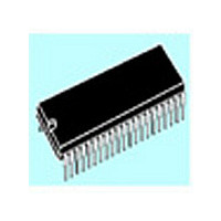
ST72T774J9B1 STMicroelectronics, ST72T774J9B1 Datasheet - Page 82

ST72T774J9B1
Manufacturer Part Number
ST72T774J9B1
Description
Manufacturer
STMicroelectronics
Datasheet
1.ST72T774J9B1.pdf
(144 pages)
Specifications of ST72T774J9B1
Cpu Family
ST7
Device Core Size
8b
Frequency (max)
24MHz
Interface Type
I2C/USB
Program Memory Type
EPROM
Program Memory Size
60KB
Total Internal Ram Size
1KB
# I/os (max)
31
Number Of Timers - General Purpose
1
Operating Supply Voltage (typ)
5V
Operating Supply Voltage (max)
5.5V
Operating Supply Voltage (min)
4V
On-chip Adc
1-chx8-bit
On-chip Dac
1-chx8-bit
Instruction Set Architecture
CISC
Operating Temp Range
0C to 70C
Operating Temperature Classification
Commercial
Mounting
Through Hole
Pin Count
42
Package Type
SPDIP
Lead Free Status / Rohs Status
Specific Sites Compliant
Available stocks
Company
Part Number
Manufacturer
Quantity
Price
Part Number:
ST72T774J9B1
Manufacturer:
ST
Quantity:
20 000
ST72774/ST727754/ST72734
USB INTERFACE (Cont’d)
Bit 0 = SOF Start of frame.
This bit is set by hardware when a low-speed SOF
indication (keep-alive strobe) is seen on the USB
bus.
Note: To avoid spurious clearing of some bits, it is recom-
INTERRUPT MASK REGISTER (IMR)
Read / Write
Reset Value: 0000 0000 (00h)
Bit 7 = Reserved. Forced by hardware to 0.
Bits 6:0 = These bits are mask bits for all interrupt
condition bits included in the ISTR. Whenever one
of the IMR bits is set, if the corresponding ISTR bit
is set, and the I bit in the CC register is cleared, an
interrupt request is generated. For an explanation
of each bit, please refer to the corresponding bit
description in ISTR.
CONTROL REGISTER (CTLR)
Read / Write
Reset Value: 0000 0110 (06h)
Bits 7:4 = Reserved. Forced by hardware to 0.
Bit 3 = RESUME Resume .
This bit is set by software to wake-up the Host
when the ST7 is in suspend mode.
82/144
7
0
0: No SOF signal detected
1: SOF signal detected
0: Resume signal not forced
1: Resume signal forced on the USB bus.
7
0
mended to clear them using a load instruction
where all bits which must not be altered are set, and
all bits to be cleared are reset. Avoid read-modify-
write instructions like AND , XOR..
0
DOV
RM
0
CTR
M
0
RESUME
ERR
M
IOVR
M
PDWN
SPM
ESU
SUSP
ETM
RES
FRES
SOF
M
0
0
Software should clear this bit after the appropriate
delay.
Bit 2 = PDWN Power down .
This bit is set by software to turn off the 3.3V on-
chip voltage regulator that supplies the external
pull-up resistor and the transceiver.
Note: After turning on the voltage regulator, software
Bit 1 = SUSP Suspend mode .
This bit is set by software to enter Suspend mode.
When the hardware detects USB activity, it resets
this bit (it can also be reset by software).
Bit 0 = FRES Force reset.
This bit is set by software to force a reset of the
USB interface, just as if a RESET sequence came
from the USB.
The USB is held in RESET state until software
clears this bit, at which point a “USB-RESET”
interrupt will be generated if enabled.
DEVICE ADDRESS REGISTER (DADDR)
Read / Write
Reset Value: 0000 0000 (00h)
Bit 7 = Reserved. Forced by hardware to 0.
Bits 6:0 = ADD[6:0] Device address, 7 bits.
Software must write into this register the address
sent by the host during enumeration.
Note: This register is also reset when a USB reset is re-
7
0
0: Voltage regulator on
1: Voltage regulator off
0: Suspend mode inactive
1: Suspend mode active
0: Reset not forced
1: USB interface reset forced.
should allow at least 3 µs for stabilisation of the
power supply before using the USB interface.
ceived from the USB bus or forced through bit
FRES in the CTLR register.
ADD6
ADD5
ADD4
ADD3
ADD2
ADD1
ADD0
0


