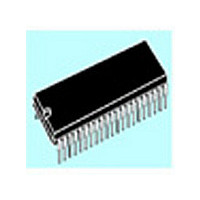
ST72T774J9B1 STMicroelectronics, ST72T774J9B1 Datasheet - Page 8

ST72T774J9B1
Manufacturer Part Number
ST72T774J9B1
Description
Manufacturer
STMicroelectronics
Datasheet
1.ST72T774J9B1.pdf
(144 pages)
Specifications of ST72T774J9B1
Cpu Family
ST7
Device Core Size
8b
Frequency (max)
24MHz
Interface Type
I2C/USB
Program Memory Type
EPROM
Program Memory Size
60KB
Total Internal Ram Size
1KB
# I/os (max)
31
Number Of Timers - General Purpose
1
Operating Supply Voltage (typ)
5V
Operating Supply Voltage (max)
5.5V
Operating Supply Voltage (min)
4V
On-chip Adc
1-chx8-bit
On-chip Dac
1-chx8-bit
Instruction Set Architecture
CISC
Operating Temp Range
0C to 70C
Operating Temperature Classification
Commercial
Mounting
Through Hole
Pin Count
42
Package Type
SPDIP
Lead Free Status / Rohs Status
Specific Sites Compliant
Available stocks
Company
Part Number
Manufacturer
Quantity
Price
Part Number:
ST72T774J9B1
Manufacturer:
ST
Quantity:
20 000
ST72774/ST727754/ST72734
PIN DESCRIPTION (Cont’d)
RESET: Bidirectional. This active low signal forces
the initialization of the MCU. This event is the top
priority non maskable interrupt. This pin is
switched low when the Watchdog has triggered or
V
peripherals.
OSCIN/OSCOUT: Input/Output Oscillator pin.
These pins connect a parallel-resonant crystal, or
an external source to the on-chip oscillator.
Table 1. ST727x4 Pin Description
8/144
3
Pin No.
39
40
41
42
43
44
1
2
3
4
5
6
8
9
10
11
12
13
14
15
16
17
DD
is low. It can be used to reset external
1
2
3
4
5
6
7
8
9
10
11
12
13
14
15
16
17
18
19
20
21
22
PC0/HSYNCDIV
PC1/AV
PC2/PWM3
PC3/PWM4
PC4/PWM5
PC5/PWM6
PC6/PWM7
PC7/PWM8
PB7/AIN3/PWM2
PB6/AIN2/PWM1
PB5/AIN1
PB4/AIN0
V
USBVCC
USBDM
USBDP
V
HSYNCI
VSYNCI
PD0/VSYNCO
PD1/HSYNCO
PD2/CSYNCI
DD
SS
Pin Name
Type
I/O
I/O
I/O
I/O
I/O
I/O
I/O
I/O
I/O
I/O
I/O
I/O
I/O
I/O
I/O
I/O
I/O
S
S
S
I
I
Port C0 or HSYNCDIV output (HSYNCO divided by 2)
Port C1 or “Active Video” input
Port C2 or 10-bit PWM/BRM output 3
Port C3 or 10-bit PWM/BRM output 4
Port C4 or 10-bit PWM/BRM output5
Port C5 or 10-bit PWM/BRM output 6
Port C6 or 10-bit PWM/BRM output 7
Port C7 or 10-bit PWM/BRM output 8
Port B7 or ADC analog input 3 or 10-bit PWM/BRM
output 2
Port B6 or ADC analog input 2 or 10-bit PWM/BRM
output 1
Port B5 or ADC analog input 1
Port B4 or ADC analog input 0
Supply (4.0V - 5.5V)
USB power supply (output 3.3V +/- 10%)
USB bidirectional data
USB bidirectional data
Ground 0V
SYNC horizontal synchronisation input
SYNC vertical synchronisation input
Port D0 or SYNC vertical synchronisation output
Port D1 or SYNC horizontal synchronisation output
Port D2 or SYNC composite synchronisation input
Description
TEST/V
This pin must be held low during normal operating
modes.
V
V
Alternate Functions: several pins of the I/O ports
assume
functions as shown in the pin description
DD
SS
: Digital Ground.
: Power supply voltage (4.0V-5.5V)
PP
: Input. EPROM programming voltage.
software
programmable
For analog controls,
after external filtering
Must be tied to ground
for devices without
USB peripheral
TTL levels
Refer to
TTL levels with pull-up
(SYNC input)
Remarks
Figure 16
alternate


