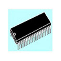
ST72T774J9B1 STMicroelectronics, ST72T774J9B1 Datasheet - Page 20

ST72T774J9B1
Manufacturer Part Number
ST72T774J9B1
Description
Manufacturer
STMicroelectronics
Datasheet
1.ST72T774J9B1.pdf
(144 pages)
Specifications of ST72T774J9B1
Cpu Family
ST7
Device Core Size
8b
Frequency (max)
24MHz
Interface Type
I2C/USB
Program Memory Type
EPROM
Program Memory Size
60KB
Total Internal Ram Size
1KB
# I/os (max)
31
Number Of Timers - General Purpose
1
Operating Supply Voltage (typ)
5V
Operating Supply Voltage (max)
5.5V
Operating Supply Voltage (min)
4V
On-chip Adc
1-chx8-bit
On-chip Dac
1-chx8-bit
Instruction Set Architecture
CISC
Operating Temp Range
0C to 70C
Operating Temperature Classification
Commercial
Mounting
Through Hole
Pin Count
42
Package Type
SPDIP
Lead Free Status / Rohs Status
Specific Sites Compliant
Available stocks
Company
Part Number
Manufacturer
Quantity
Price
Part Number:
ST72T774J9B1
Manufacturer:
ST
Quantity:
20 000
ST72774/ST727754/ST72734
3.2 RESET
The Reset procedure is used to provide an orderly
software start-up or to quit low power modes.
Five conditions generate a reset:
A reset causes the reset vector to be fetched from
addresses FFFEh and FFFFh in order to be loaded
into the PC and with program execution starting
from this point.
An internal circuitry provides a 4096 CPU clock
cycle delay from the time that the oscillator
becomes active.
3.2.1 LVD and Watchdog Reset
The Low Voltage Detector (LVD) generates a reset
when V
when
is active only when V
During LVD Reset, the RESET pin is held low, thus
permitting the MCU to reset other devices.
Table 5. List of sections affected by RESET and WAIT (Refer to 3.6 for Wait Mode)
20/144
Fast bit of the miscellaneous register set to one (24 MHz as external clock)
Timer Prescaler reset to zero
Timer Counter set to FFFCh
All Timer enable bits set to 0 (disabled)
Data Direction Registers set to 0 (as Inputs)
Set Stack Pointer to 01FFh
Force Internal Address Bus to restart vector FFFEh, FFFFh
Set Interrupt Mask Bit (I-Bit, CC) to 1 (Interrupt disable)
Set Interrupt Mask Bit (I-Bit, CC) to 0 (Interrupt enable)
Reset WAIT latch
Disable Oscillator (for 4096 cycles)
Set Timer Clock to 0
Watchdog counter reset
Watchdog register reset
Port data registers reset
Other on-chip peripherals: registers reset
LVD,
watchdog,
external pulse at the RESET pin,
illegal address,
illegal opcode.
VDD
DD
is falling (refer to
is below V
TRH
DD
when V
is above V
Figure
Section
DD
11). This circuitry
is rising or V
TRM.
TRL
When a watchdog reset occurs, the RESET pin is
pulled low permitting the MCU to reset other
devices as when Power on/off
3.2.2 External Reset
The external reset is an active low input signal
applied to the RESET pin of the MCU.
As shown in
remain low for 1000ns.
An internal Schmitt trigger at the RESET pin is
provided to improve noise immunity.
3.2.3 Illegal Address Detection
An opcode fetch from an illegal address (refer to
Figure
Program
forbidden (especially to protect page 0 registers
against spurious accesses).
3.2.4 Illegal Opcode Detection
Illegal instructions corresponding to no valid
opcode
Programming Manual.
3) generates an illegal address reset.
generate
execution
Figure
X
X
X
X
X
X
X
X
X
X
X
X
X
X
X
RESET
12, the RESET signal must
a
at
reset.
those
X
(Figure
WAIT
Refer
addresses
10).
to
ST7
is


