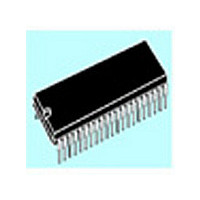
ST72T774J9B1 STMicroelectronics, ST72T774J9B1 Datasheet - Page 56

ST72T774J9B1
Manufacturer Part Number
ST72T774J9B1
Description
Manufacturer
STMicroelectronics
Datasheet
1.ST72T774J9B1.pdf
(144 pages)
Specifications of ST72T774J9B1
Cpu Family
ST7
Device Core Size
8b
Frequency (max)
24MHz
Interface Type
I2C/USB
Program Memory Type
EPROM
Program Memory Size
60KB
Total Internal Ram Size
1KB
# I/os (max)
31
Number Of Timers - General Purpose
1
Operating Supply Voltage (typ)
5V
Operating Supply Voltage (max)
5.5V
Operating Supply Voltage (min)
4V
On-chip Adc
1-chx8-bit
On-chip Dac
1-chx8-bit
Instruction Set Architecture
CISC
Operating Temp Range
0C to 70C
Operating Temperature Classification
Commercial
Mounting
Through Hole
Pin Count
42
Package Type
SPDIP
Lead Free Status / Rohs Status
Specific Sites Compliant
Available stocks
Company
Part Number
Manufacturer
Quantity
Price
Part Number:
ST72T774J9B1
Manufacturer:
ST
Quantity:
20 000
ST72774/ST727754/ST72734
4.4 SYNC PROCESSOR (SYNC)
4.4.1 Introduction
The Sync processor handles all the management
tasks of the video synchronization signals, and is
used with the timer and software to provide
information and status on the video standard and
timings. This block supports multiple video
standards such as: Separate Sync, Composite
Sync and (via an external extractor) Sync on
Green. The internal clock in the Sync processor is
4 MHz.
4.4.2 Main Features
– Presence of incoming signals (edge detection)
– Read the HSYNCI / VSYNCI input signal levels
– Measure the signal periods
– Detect the sync polarities
– Detect the composite sync and extract VSYNCO
Figure 37. Sync Processor Block Diagram
56/144
VSYNCI1
VSYNCI2
HSYNCI1
HSYNCI2
CSYNCI
Note: CLK is f
Input Processing
Output Processing
Pull-Up Resistor (if existing)
HVSEL
1
0
0
1
HVSEL
INT/2
Pulse Detect
Pulse Detect
in fast mode (see note in Clock System section)
Latch
Pulse Detect
Latch
Latch
0
1
SCI0
HSYNCI / CSYNCI
Detect
LCV0
Sync
Edge
&
Prescaler
LD
PSCD
(see note)
VSYNCI
Capture
Register
f
INT
Up / Down
CLK
ICAP2 TIMER
5-Bit Counter
match
Latch
00
Control
LCV1
Logic
Correction
H Sync O
match
H Sync O
Latch
H-Inhibit
ON/OFF
Polarity
1F
EN
Vsync*
– Control the sync output polarities
– Generate free-running frequencies
– Generate a video blanking signal
– Generate a clamping signal or a Moire signal
– Measure the number of scan lines per frame to
– Detect HSYNCI reaching too high a frequency
– Detect pre/post equalization pulses
– Measure the low level of HSYNCO or HFBACK
– Inhibit Pre/Post equalization pulses
– Program VSYNCO pulse width extension
– Extend VSYNCO pulse widths during:
Note: Some external pins are not available on all devices.
simplify OSD vertical centering
Analyzer Mode
Corrector Mode
V
S
Y
N
C
O
LCV1
HFBACK
post-equalization pulse detection only
pre and post-equalization pulse detection
Refer to the device pinout description.
HVGEN
0
1
VFBACK
FBSEL
VFBACK
V Sync O
ICAP1 TIMER
1
HFBACK
0
Polarity
Back Porch
Generator
Sync Generator
Clamp
Hardware Block
(Positive polarity)
Sync Corrector
Sync Analyzer
FBSEL
1
0
Correction
Detector
Polarity
V Sync
Other
CLPINV
Polarity
Clamp
SYNOP
BP1, BP0
00
0
1
HVGEN
VSYNC Generator
Typical Pulse Width
HSYNC Generator
Generator
Blanking
Duty cycle range
CLMPEN
40 - 200 Hz
20 - 256 µs
15 - 200 kHz
3 - 40 %
SYNOP
BLKEN
HSYNCO
CLAMPOUT
BLANKOUT
VR02071C
VSYNCO


