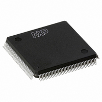
SAA7146AH/V4,557 NXP Semiconductors, SAA7146AH/V4,557 Datasheet - Page 130

SAA7146AH/V4,557
Manufacturer Part Number
SAA7146AH/V4,557
Description
IC VIDEO SPCI BRIDGE HP 160-QFP
Manufacturer
NXP Semiconductors
Type
Video Bridger
Datasheet
1.SAA7146AHV4557.pdf
(139 pages)
Specifications of SAA7146AH/V4,557
Package / Case
160-QFP
Applications
DTV
Mounting Type
Surface Mount
Maximum Operating Temperature
+ 70 C
Minimum Operating Temperature
0 C
Mounting Style
SMD/SMT
Lead Free Status / RoHS Status
Lead free / RoHS Compliant
Lead Free Status / RoHS Status
Lead free / RoHS Compliant, Lead free / RoHS Compliant
Other names
568-1318
935269343557
SAA7146AHBB
935269343557
SAA7146AHBB
Available stocks
Company
Part Number
Manufacturer
Quantity
Price
Company:
Part Number:
SAA7146AH/V4,557
Manufacturer:
NXP Semiconductors
Quantity:
10 000
- Current page: 130 of 139
- Download datasheet (576Kb)
Philips Semiconductors
Notes
1. Input leakage currents include high-impedance output leakage for all bidirectional buffer with 3-state outputs.
2. Levels measured with load circuit: 1.2 k at 3 V (TTL load) and C
3. Voltage of the V
4. C
5. I/O pins of fast-mode devices must not obstruct the SDA and SCL lines if V
6. FRAME#, TRDY#, IRDY#, DEVSEL# and STOP#.
7. Lower capacitance on this input only pin allows for non-resistive coupling to AD(xx).
8. Refer to the V/I curves in PCI specification. ‘Switching current high’ specifications are not relevant to INTA#, which
9. I
10. I
11. This parameter is to be interpreted as the cumulative edge rate across the specified range, rather than the
12. REQ# and GNT# are point-to-point signals, and have different output valid delay and input set-up times that do
13. For purposes of active/float timing measurements the high-impedance or ‘off’ state is defined to be when the total
14. RST# is asserted and de-asserted asynchronously with respect to CLK.
15. All output drivers floated asynchronously when RST# is active.
2004 Aug 25
t
t
t
t
t
t
SYMBOL
off
su
su(ptp)
h
rst(CLK)
rst(off)
Multimedia bridge, high performance
Scaler and PCI circuit (SPCI)
and V
are open-drain outputs.
instantaneous rate at any point within the transition range.
bussed signals. GNT# has a set-up time of 10 ns. REQ# has an output valid delay time of 12 ns. All other signals are
bussed.
current delivered through the component pin is less than or equal to the leakage current specification.
OH
OL
b
= capacitance of one bus line measured in pF.
= 78.5
= 11.9
DDI2C
active to float delay
input set-up time to CLK
(bussed signal)
input set-up time to CLK
(point-to-point)
input hold time from CLK
reset active time after CLK stable
reset active to output float delay
(3.0 : 3.3 : 3.6) (MIN. : TYP. : MAX.) for 3 V I
V
(V
o
o
DDI2C
(4.4
5.25)
PARAMETER
sense pin is defined as V
V
o
(V
) for 0 V < V
o
+ 2.45) for V
o
< 0.71 V.
DDD
see note 13 and
Fig.47
see note 12 and
Fig.47
see note 12
and Fig.47
see Fig.47
note 14
notes 13,
14 and 15
CONDITIONS
DDI2C
> V
o
> 3.1 V.
(4.75 : 5.0 : 5.25) (MIN. : TYP. : MAX.) for 5 V I
130
2
C-bus devices.
7
10, 12
0
100
L
= 40 pF.
MIN.
DDI2C
is switched off.
TYP.
28
40
Product specification
SAA7146A
MAX.
2
C-bus devices
UNIT
ns
ns
ns
ns
ns
s
Related parts for SAA7146AH/V4,557
Image
Part Number
Description
Manufacturer
Datasheet
Request
R
Part Number:
Description:
Manufacturer:
NXP Semiconductors
Datasheet:

Part Number:
Description:
Manufacturer:
NXP Semiconductors
Datasheet:
Part Number:
Description:
NXP Semiconductors designed the LPC2420/2460 microcontroller around a 16-bit/32-bitARM7TDMI-S CPU core with real-time debug interfaces that include both JTAG andembedded trace
Manufacturer:
NXP Semiconductors
Datasheet:

Part Number:
Description:
NXP Semiconductors designed the LPC2458 microcontroller around a 16-bit/32-bitARM7TDMI-S CPU core with real-time debug interfaces that include both JTAG andembedded trace
Manufacturer:
NXP Semiconductors
Datasheet:
Part Number:
Description:
NXP Semiconductors designed the LPC2468 microcontroller around a 16-bit/32-bitARM7TDMI-S CPU core with real-time debug interfaces that include both JTAG andembedded trace
Manufacturer:
NXP Semiconductors
Datasheet:
Part Number:
Description:
NXP Semiconductors designed the LPC2470 microcontroller, powered by theARM7TDMI-S core, to be a highly integrated microcontroller for a wide range ofapplications that require advanced communications and high quality graphic displays
Manufacturer:
NXP Semiconductors
Datasheet:
Part Number:
Description:
NXP Semiconductors designed the LPC2478 microcontroller, powered by theARM7TDMI-S core, to be a highly integrated microcontroller for a wide range ofapplications that require advanced communications and high quality graphic displays
Manufacturer:
NXP Semiconductors
Datasheet:
Part Number:
Description:
The Philips Semiconductors XA (eXtended Architecture) family of 16-bit single-chip microcontrollers is powerful enough to easily handle the requirements of high performance embedded applications, yet inexpensive enough to compete in the market for hi
Manufacturer:
NXP Semiconductors
Datasheet:
Part Number:
Description:
The XA-S3 device is a member of Philips Semiconductors? XA(eXtended Architecture) family of high performance 16-bitsingle-chip microcontrollers
Manufacturer:
NXP Semiconductors
Datasheet:

Part Number:
Description:
The NXP BlueStreak LH75401/LH75411 family consists of two low-cost 16/32-bit System-on-Chip (SoC) devices
Manufacturer:
NXP Semiconductors
Datasheet:

Part Number:
Description:
The NXP LPC3130/3131 combine an 180 MHz ARM926EJ-S CPU core, high-speed USB2
Manufacturer:
NXP Semiconductors
Datasheet:

Part Number:
Description:
The NXP LPC3141 combine a 270 MHz ARM926EJ-S CPU core, High-speed USB 2
Manufacturer:
NXP Semiconductors

Part Number:
Description:
The NXP LPC3143 combine a 270 MHz ARM926EJ-S CPU core, High-speed USB 2
Manufacturer:
NXP Semiconductors

Part Number:
Description:
The NXP LPC3152 combines an 180 MHz ARM926EJ-S CPU core, High-speed USB 2
Manufacturer:
NXP Semiconductors


