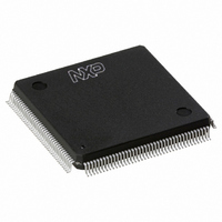
SAA7146AH/V4,557 NXP Semiconductors, SAA7146AH/V4,557 Datasheet - Page 81

SAA7146AH/V4,557
Manufacturer Part Number
SAA7146AH/V4,557
Description
IC VIDEO SPCI BRIDGE HP 160-QFP
Manufacturer
NXP Semiconductors
Type
Video Bridger
Datasheet
1.SAA7146AHV4557.pdf
(139 pages)
Specifications of SAA7146AH/V4,557
Package / Case
160-QFP
Applications
DTV
Mounting Type
Surface Mount
Maximum Operating Temperature
+ 70 C
Minimum Operating Temperature
0 C
Mounting Style
SMD/SMT
Lead Free Status / RoHS Status
Lead free / RoHS Compliant
Lead Free Status / RoHS Status
Lead free / RoHS Compliant, Lead free / RoHS Compliant
Other names
568-1318
935269343557
SAA7146AHBB
935269343557
SAA7146AHBB
Available stocks
Company
Part Number
Manufacturer
Quantity
Price
Company:
Part Number:
SAA7146AH/V4,557
Manufacturer:
NXP Semiconductors
Quantity:
10 000
Philips Semiconductors
7.12.4
The BRS programming has in principle three modes:
1. Inbound and downscaling: the binary ratio scaler input multiplexer selects data from the Dual D1 real time video
2. Outbound and upscaling in direct and line memory mode: the binary ratio scaler takes the data from FIFO 3.
3. Outbound and upscaling in field memory mode: the binary ratio scaler takes the data from FIFO 3. The DMA3 is
Table 69 BRS control register
2004 Aug 25
58
OFFSET
Multimedia bridge, high performance
Scaler and PCI circuit (SPCI)
(HEX)
interface, Port A or B and ‘normally’ writes the result via FIFO 3 and DMA3 to PCI, if DMA3 is enabled in master write
mode and not used for other purposes. Syncs including Field ID are taken from Port A or B (FID defines which base
address is used in DMA3).
The DMA3 is in master read operation. The scaling result can be selected by the DD1 port output multiplexers.
The timing reference signals (VS, HS, LLC and FID) are taken from Port A or B.
in master read operation. The scaling result can be selected by the DD1 port output multiplexers. The vertical sync
signal is taken from the VS_A or VS_B port as timing reference signal. At the HS_A or HS_B port the SAA7146A
generates a reset signal for each field. The PXQ is an output signal which is connected to the write enable port of
the memory. If an interlaced source is selected (different base addresses for ODD and EVEN fields), the field
detection must be set to ‘free toggle’ mode, due to the missing horizontal sync signal.
BRS P
BRSdatasel
and MODE
BRSsyncsel
BYO
BRS_V
ROGRAMMING
NAME
31 and 30 RW
29
28 to 19
18 and 17 RW
R
EGISTER
BIT
RW
RW
TYPE
source select for BRS video data:
source select for BRS sync signals:
vertical offset, counted in lines,
after selected vertical sync edge
until data is captured from DD1
vertical downscaling:
00: video data stream from A
01: video data stream from B
10: reserved
0: take Ha, Va, Fa, LLC_A as
select in the ‘Initial setting of
Dual D1 Interface’;
see Table 66.
1: take Hb, Vb, Fb, LLC_B as
select in the ‘Initial Setting of
Dual D1 Interface’;
see Table 66.
00: write every line to DMA3
01: write every 2nd line only
10: reserved
11: write every 4th line only
81
INBOUND
DESCRIPTION
in direct and line memory mode
the same setting as in the
inbound mode is select
in field memory mode the
horizontal sync port must set to
output to get the a field RESET
signal for a field memory
BYO defines a vertical offset,
counted in lines, after selected
vertical sync-edge until data is
read from the FIFO. For field
memory mode BYO must be
000H. The video window is
selected by ‘NumLines’,
‘NumBytes’, ‘pitch’ and ‘base
address’.
vertical upscaling:
11: read from DMA_3/FIFO 3
00: regular read
01: read every line twice
10: reserved
11: read every line 4 times
OUTBOUND
Product specification
SAA7146A


