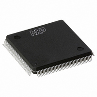
SAA7146AH/V4,557 NXP Semiconductors, SAA7146AH/V4,557 Datasheet - Page 20

SAA7146AH/V4,557
Manufacturer Part Number
SAA7146AH/V4,557
Description
IC VIDEO SPCI BRIDGE HP 160-QFP
Manufacturer
NXP Semiconductors
Type
Video Bridger
Datasheet
1.SAA7146AHV4557.pdf
(139 pages)
Specifications of SAA7146AH/V4,557
Package / Case
160-QFP
Applications
DTV
Mounting Type
Surface Mount
Maximum Operating Temperature
+ 70 C
Minimum Operating Temperature
0 C
Mounting Style
SMD/SMT
Lead Free Status / RoHS Status
Lead free / RoHS Compliant
Lead Free Status / RoHS Status
Lead free / RoHS Compliant, Lead free / RoHS Compliant
Other names
568-1318
935269343557
SAA7146AHBB
935269343557
SAA7146AHBB
Available stocks
Company
Part Number
Manufacturer
Quantity
Price
Company:
Part Number:
SAA7146AH/V4,557
Manufacturer:
NXP Semiconductors
Quantity:
10 000
Philips Semiconductors
7.2.3
The SAA7146A provides up to four audio DMA channels,
each using a FIFO of 24 Dwords. Two channels are read
only (A1_in and A2_in) and two channels are write only
(A1_out and A2_out). Because audio represents a
continuous data stream, which is neither line nor field
dependent, the audio DMA control offers only one base
address (BaseAxx) and no pitch register. For FIFO
overflow and underflow the handling of these channels is
done in the same way as the video DMA channels
(see Section 7.2.2).
Table 5 Audio DMA control register
2004 Aug 25
94
98
9C
A0
A4
A8
OFFSET
Multimedia bridge, high performance
Scaler and PCI circuit (SPCI)
(HEX)
A
UDIO
BaseA1_in
ProtA1_in
PageA1_in
MEA1_in
LimitA1_in
PVA1_in
BaseA1_out
ProtA1_out
PageA1_out
MEA1_out
LimitA1_out
PVA1_out
DMA
NAME
CONTROL
31 to 0
31 to 2
1 to 0
31 to 12
11
10 to 8
7 to 4
3
2 to 0
31 to 0
31 to 2
1 and 0
31 to 12
11
10 to 8
7 to 4
3
2 to 0
BIT
RW
RW
RW
RW
RW
RW
RW
RW
RW
RW
RW
RW
TYPE
base address for audio input Channel 1; this value specifies a
byte address
protection address for audio input Channel 1; this address
could be used to specify a upper limit for audio access in memory
space
reserved
base address of the page table, see Section 7.2.4.
mapping enable; this bit enables the MMU
reserved
interrupt limit; defines the size of the memory range, that
generates an interrupt, if its boundaries are passed
protection violation handling
reserved
Base address for audio output Channel 1; this value specifies a
byte address. The lower two bits are forced to zero.
protection address for audio output Channel 1; this address
could be used to specify a upper limit for audio access in memory
space
reserved
base address of the page table, see Section 7.2.4.
mapping enable; this bit enables the MMU
reserved
interrupt limit; defines the size of the memory range, that
generates an interrupt, if its boundaries are passed
protection violation handling
reserved
20
The protection violation handling differs only if the limit
register and the PV bit are programmed to zero. The audio
DMA channel does not wait for the EOF signal, like the
video ones. It does not generate interrupts. The interrupt
range specified by the limit register is defined in the same
way as described in Section 7.2.2. The audio DMA
channels try immediately to transfer data after setting the
transfer enable bits. All registers for audio DMA control,
which are the base address, the protection address and
the control bits are listed in the following Table 5, except
the input control bits (Burst, Threshold), which are listed in
Table 6.
DESCRIPTION
Product specification
SAA7146A


