SAA7146AH/V4,557 NXP Semiconductors, SAA7146AH/V4,557 Datasheet - Page 17
SAA7146AH/V4,557
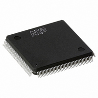
Manufacturer Part Number
SAA7146AH/V4,557
Description
IC VIDEO SPCI BRIDGE HP 160-QFP
Manufacturer
NXP Semiconductors
Type
Video Bridger
Datasheet
1.SAA7146AHV4557.pdf
(139 pages)
Specifications of SAA7146AH/V4,557
Package / Case
160-QFP
Applications
DTV
Mounting Type
Surface Mount
Maximum Operating Temperature
+ 70 C
Minimum Operating Temperature
0 C
Mounting Style
SMD/SMT
Lead Free Status / RoHS Status
Lead free / RoHS Compliant
Lead Free Status / RoHS Status
Lead free / RoHS Compliant, Lead free / RoHS Compliant
Other names
568-1318
935269343557
SAA7146AHBB
935269343557
SAA7146AHBB
Available stocks
Company
Part Number
Manufacturer
Quantity
Price
Company:

Part Number:
SAA7146AH/V4,557
Manufacturer:
NXP Semiconductors
Quantity:
10 000


Philips Semiconductors
2004 Aug 25
OFFSET
28
2C
30
34
38
3C
40
44
(HEX)
Multimedia bridge, high performance
Scaler and PCI circuit (SPCI)
RW2
Swap2
NumLines2 27 to 16 RW
NumBytes2 11 to 0
BaseOdd3
BaseEven3 31 to 0
ProtAddr3
Pitch3
Page3
ME3
Limit3
PV3
RW3
Swap3
NumLines3 27 to 16 RW
NumBytes3 11 to 0
NAME
2
1 and 0
31 to 0
31 to 2
1 and 0
31 to 0
31 to 12 RW
11
10 to 8
7 to 4
3
2
1 and 0
BIT
RW
RW
RW
RW
RW
RW
RW
RW
RW
RW
RW
RW
RW
TYPE
Specifies the data stream direction of FIFO 2. A logic 0 enables a write
operation to the PCI memory. A logic 1 enables a read operation from the
PCI memory.
endian swapping of all Dwords passing the FIFO 2:
Number of lines per field: in read mode NumLines defines the number of
lines to be read from system memory. A logic 0 specifies one line. In write
mode this register is not used.
Number of bytes per line: in read mode this defines the number of bytes
per line to be read from system memory. A logic 0 specifies one byte. In
write mode this register is not used.
PCI base address for odd fields of the upper (or lower if top-down flip is
selected) left pixel of the transferred field
PCI base address for even fields of the upper (or lower if top-down flip is
selected) left pixel of the transferred field
protection address
reserved
distance between the start addresses of two consecutive lines of a field
base address of the page table (see Section 7.2.4)
mapping enable; this bit enables the MMU
reserved
interrupt limit; defines the size of the memory range, that raise an
interrupt, if its boundaries are passed
protection violation handling
Specifies the data stream direction of FIFO 3. A logic 0 enables a write
operation to the PCI memory. A logic 1 enables a read operation from the
PCI memory.
endian swapping of all Dwords passing the FIFO 3:
Number of lines per field: in read mode NumLines defines the number of
lines to be read from system memory. A logic 0 specifies one line. In write
mode it defines the number of qualified lines to be processed by the BRS
per field. This will cut off all the following input-lines at the BRS input.
Number of bytes per line: in read mode this defines the number of bytes
per line to be read from system memory. A logic 0 specifies one byte. In
write mode it defines the number of qualified bytes to be processed by the
BRS per line. This will cut off all the following bytes at the BRS input.
00 = no swap
01 = 2-byte swap (3210 to 2301)
10 = 4-byte swap (3210 to 0123)
11 = reserved
00 = no swap
01 = 2-byte swap (3210 to 2301)
10 = 4-byte swap (3210 to 0123)
11 = reserved
17
DESCRIPTION
Product specification
SAA7146A
Related parts for SAA7146AH/V4,557
Image
Part Number
Description
Manufacturer
Datasheet
Request
R

Part Number:
Description:
Manufacturer:
NXP Semiconductors
Datasheet:

Part Number:
Description:
Manufacturer:
NXP Semiconductors
Datasheet:
Part Number:
Description:
NXP Semiconductors designed the LPC2420/2460 microcontroller around a 16-bit/32-bitARM7TDMI-S CPU core with real-time debug interfaces that include both JTAG andembedded trace
Manufacturer:
NXP Semiconductors
Datasheet:

Part Number:
Description:
NXP Semiconductors designed the LPC2458 microcontroller around a 16-bit/32-bitARM7TDMI-S CPU core with real-time debug interfaces that include both JTAG andembedded trace
Manufacturer:
NXP Semiconductors
Datasheet:
Part Number:
Description:
NXP Semiconductors designed the LPC2468 microcontroller around a 16-bit/32-bitARM7TDMI-S CPU core with real-time debug interfaces that include both JTAG andembedded trace
Manufacturer:
NXP Semiconductors
Datasheet:
Part Number:
Description:
NXP Semiconductors designed the LPC2470 microcontroller, powered by theARM7TDMI-S core, to be a highly integrated microcontroller for a wide range ofapplications that require advanced communications and high quality graphic displays
Manufacturer:
NXP Semiconductors
Datasheet:
Part Number:
Description:
NXP Semiconductors designed the LPC2478 microcontroller, powered by theARM7TDMI-S core, to be a highly integrated microcontroller for a wide range ofapplications that require advanced communications and high quality graphic displays
Manufacturer:
NXP Semiconductors
Datasheet:
Part Number:
Description:
The Philips Semiconductors XA (eXtended Architecture) family of 16-bit single-chip microcontrollers is powerful enough to easily handle the requirements of high performance embedded applications, yet inexpensive enough to compete in the market for hi
Manufacturer:
NXP Semiconductors
Datasheet:
Part Number:
Description:
The XA-S3 device is a member of Philips Semiconductors? XA(eXtended Architecture) family of high performance 16-bitsingle-chip microcontrollers
Manufacturer:
NXP Semiconductors
Datasheet:

Part Number:
Description:
The NXP BlueStreak LH75401/LH75411 family consists of two low-cost 16/32-bit System-on-Chip (SoC) devices
Manufacturer:
NXP Semiconductors
Datasheet:
Part Number:
Description:
The NXP LPC3130/3131 combine an 180 MHz ARM926EJ-S CPU core, high-speed USB2
Manufacturer:
NXP Semiconductors
Datasheet:
Part Number:
Description:
The NXP LPC3141 combine a 270 MHz ARM926EJ-S CPU core, High-speed USB 2
Manufacturer:
NXP Semiconductors
Part Number:
Description:
The NXP LPC3143 combine a 270 MHz ARM926EJ-S CPU core, High-speed USB 2
Manufacturer:
NXP Semiconductors

Part Number:
Description:
The NXP LPC3152 combines an 180 MHz ARM926EJ-S CPU core, High-speed USB 2
Manufacturer:
NXP Semiconductors