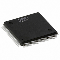
SAA7146AH/V4,557 NXP Semiconductors, SAA7146AH/V4,557 Datasheet - Page 26

SAA7146AH/V4,557
Manufacturer Part Number
SAA7146AH/V4,557
Description
IC VIDEO SPCI BRIDGE HP 160-QFP
Manufacturer
NXP Semiconductors
Type
Video Bridger
Datasheet
1.SAA7146AHV4557.pdf
(139 pages)
Specifications of SAA7146AH/V4,557
Package / Case
160-QFP
Applications
DTV
Mounting Type
Surface Mount
Maximum Operating Temperature
+ 70 C
Minimum Operating Temperature
0 C
Mounting Style
SMD/SMT
Lead Free Status / RoHS Status
Lead free / RoHS Compliant
Lead Free Status / RoHS Status
Lead free / RoHS Compliant, Lead free / RoHS Compliant
Other names
568-1318
935269343557
SAA7146AHBB
935269343557
SAA7146AHBB
Available stocks
Company
Part Number
Manufacturer
Quantity
Price
Company:
Part Number:
SAA7146AH/V4,557
Manufacturer:
NXP Semiconductors
Quantity:
10 000
- Current page: 26 of 139
- Download datasheet (576Kb)
Philips Semiconductors
7.2.6
Table 9 lists the status information that the PCI interface makes available to the user in addition to the interrupt sources
that are described later. This information is read only.
Table 9 Status bits of the DMA control
7.3
7.3.1
The SAA7146A has two Dwords of general control to
support quick enable/disable switching of any activity of
the SAA7146A via direct access by the CPU. These main
control Dwords are split in two parts. The upper parts have
16 bits of bit-mask to allow bit-selective write to the lower
part which contains single bit enable/disable control of
major interface functions of SAA7146A. If a certain bit
position is masked with a logic 1 in the mask word (upper
2 bytes) during a write access, then the corresponding bit
in the control word (lower 2 bytes) is changed according to
the contents of the transmitted data. By that the CPU can
easily switch on or off certain selected interfaces of the
SAA7146A without checking the actual ‘remaining’
programming (enabling) of the other parts.
2004 Aug 25
120
124
128
12C
130
134
138
13C
Multimedia bridge, high performance
Scaler and PCI circuit (SPCI)
OFFSET
(HEX)
Main control
S
G
TATUS INFORMATION OF THE
ENERAL
PCI_VDP1
PCI_VDP2
PCI_VDP3
PCI_ADP1
PCI_ADP2
PCI_ADP3
PCI_ADP4
PCI_DDP
NAME
31 to 0
31 to 0
31 to 0
31 to 0
31 to 0
31 to 0
31 to 0
31 to 0
BIT
PCI
INTERFACE
R
R
R
R
R
R
R
R
TYPE
26
logical video DMA pointer of FIFO 1
logical video DMA pointer of FIFO 2
logical video DMA pointer of FIFO 3
logical audio DMA pointer of audio output FIFO A1_out
logical audio DMA pointer of audio input FIFO A1_in
logical audio DMA pointer of audio output FIFO A2_out
logical audio DMA pointer of audio input FIFO A2_in
logical DEBI DMA pointer
The programming of registers for the 3 Video DMA
channels, both video processors (HPS, BRS) and for the
interfaces DEBI and I
method. This is done to guarantee coherent programming
data. During initiation of an upload operation from a
shadow RAM each of the UPLD bits [10 to 0] (see
Table 11) is assigned to a set of registers. If a logic 1 is
written into a UPLD bit all dedicated shadow RAM
registers containing changed data are uploaded into their
working registers immediately. During a read cycle the
UPLD bits give information on whether the shadow RAM
contains changed data not yet uploaded into the working
registers. The UPLD bits remain HIGH as long as the
contents of the shadow RAM represents the current
programming.
DESCRIPTION
2
C-bus is performed by an upload
Product specification
SAA7146A
Related parts for SAA7146AH/V4,557
Image
Part Number
Description
Manufacturer
Datasheet
Request
R
Part Number:
Description:
Manufacturer:
NXP Semiconductors
Datasheet:

Part Number:
Description:
Manufacturer:
NXP Semiconductors
Datasheet:
Part Number:
Description:
NXP Semiconductors designed the LPC2420/2460 microcontroller around a 16-bit/32-bitARM7TDMI-S CPU core with real-time debug interfaces that include both JTAG andembedded trace
Manufacturer:
NXP Semiconductors
Datasheet:

Part Number:
Description:
NXP Semiconductors designed the LPC2458 microcontroller around a 16-bit/32-bitARM7TDMI-S CPU core with real-time debug interfaces that include both JTAG andembedded trace
Manufacturer:
NXP Semiconductors
Datasheet:
Part Number:
Description:
NXP Semiconductors designed the LPC2468 microcontroller around a 16-bit/32-bitARM7TDMI-S CPU core with real-time debug interfaces that include both JTAG andembedded trace
Manufacturer:
NXP Semiconductors
Datasheet:
Part Number:
Description:
NXP Semiconductors designed the LPC2470 microcontroller, powered by theARM7TDMI-S core, to be a highly integrated microcontroller for a wide range ofapplications that require advanced communications and high quality graphic displays
Manufacturer:
NXP Semiconductors
Datasheet:
Part Number:
Description:
NXP Semiconductors designed the LPC2478 microcontroller, powered by theARM7TDMI-S core, to be a highly integrated microcontroller for a wide range ofapplications that require advanced communications and high quality graphic displays
Manufacturer:
NXP Semiconductors
Datasheet:
Part Number:
Description:
The Philips Semiconductors XA (eXtended Architecture) family of 16-bit single-chip microcontrollers is powerful enough to easily handle the requirements of high performance embedded applications, yet inexpensive enough to compete in the market for hi
Manufacturer:
NXP Semiconductors
Datasheet:
Part Number:
Description:
The XA-S3 device is a member of Philips Semiconductors? XA(eXtended Architecture) family of high performance 16-bitsingle-chip microcontrollers
Manufacturer:
NXP Semiconductors
Datasheet:

Part Number:
Description:
The NXP BlueStreak LH75401/LH75411 family consists of two low-cost 16/32-bit System-on-Chip (SoC) devices
Manufacturer:
NXP Semiconductors
Datasheet:

Part Number:
Description:
The NXP LPC3130/3131 combine an 180 MHz ARM926EJ-S CPU core, high-speed USB2
Manufacturer:
NXP Semiconductors
Datasheet:

Part Number:
Description:
The NXP LPC3141 combine a 270 MHz ARM926EJ-S CPU core, High-speed USB 2
Manufacturer:
NXP Semiconductors

Part Number:
Description:
The NXP LPC3143 combine a 270 MHz ARM926EJ-S CPU core, High-speed USB 2
Manufacturer:
NXP Semiconductors

Part Number:
Description:
The NXP LPC3152 combines an 180 MHz ARM926EJ-S CPU core, High-speed USB 2
Manufacturer:
NXP Semiconductors


