DEMO9RS08KA2 Freescale Semiconductor, DEMO9RS08KA2 Datasheet - Page 112
DEMO9RS08KA2
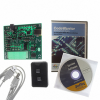
Manufacturer Part Number
DEMO9RS08KA2
Description
DEMO BOARD FOR 9RS08KA2
Manufacturer
Freescale Semiconductor
Series
RS08r
Type
MCUr
Datasheets
1.DEMO9RS08KA2.pdf
(136 pages)
2.DEMO9RS08KA2.pdf
(28 pages)
3.DEMO9RS08KA2.pdf
(2 pages)
4.DEMO9RS08KA2.pdf
(6 pages)
Specifications of DEMO9RS08KA2
Contents
Board, Cable, CD, Documentation, Sample ICs
Processor To Be Evaluated
RS08KA2
Data Bus Width
8 bit
Interface Type
USB
Silicon Manufacturer
Freescale
Core Architecture
RS08
Core Sub-architecture
RS08
Silicon Core Number
MC9RS08
Silicon Family Name
RS08KA
Rohs Compliant
Yes
For Use With/related Products
MC9RS08KA2
Lead Free Status / RoHS Status
Lead free / RoHS Compliant
Available stocks
Company
Part Number
Manufacturer
Quantity
Price
Company:

Part Number:
DEMO9RS08KA2
Manufacturer:
Freescale Semiconductor
Quantity:
135


Appendix A Electrical Characteristics
112
1
2
3
4
5
6
Input low voltage (V
Input low voltage (1.8 V ≤ V
Input hysteresis (all digital inputs)
Input leakage current (per pin)
High impedance (off-state) leakage current (per pin)
Internal pullup/pulldown resistors
Output high voltage (port A)
Maximum total I
Output low voltage (port A)
Maximum total I
dc injection current
Input capacitance (all non-supply pins)
This parameter is characterized and not tested on each device.
Measurement condition for pull resistors: V
All functional non-supply pins are internally clamped to V
V
Input must be current limited to the value specified. To determine the value of the required current-limiting resistor, calculate
resistance values for positive and negative clamp voltages, then use the larger of the two values.
Power supply must maintain regulation within operating V
conditions. If positive injection current (V
in external power supply going out of regulation. Ensure external V
current. This will be the greatest risk when the MCU is not consuming power. Examples are: if no system clock is present, or
if clock rate is very low which would reduce overall power consumption.
This parameter is characterized and not tested on each device.
(all digital inputs)
I
I
I
I
I
Single pin limit
Total MCU limit, includes sum of all stressed pins
I
SS
OH
OH
OH
OL
OL
V
V
OL
In
In
only.
V
= 3 mA (V
= 2 mA (V
= 5 mA (V
= –5 mA (V
= –3 mA (V
= –2 mA (V
= V
= V
In
< V
DD
DD
SS
or V
or V
, V
OH
OL
DD
DD
DD
SS
SS,
DD
DD
DD
In
for all port pins
for all port pins
≥ 3 V)
≥ 1.8 V)
3, 4, 5 6
DD
, all input/output
≥ 4.5 V)
> V
all input only pins
≥ 4.5 V)
≥ 3 V)
≥ 1.8 V)
Parameter
> 2.3 V) (all digital inputs)
DD
DD
≤ 2.3 V)
2
(all port pins)
(Temperature Range = –40 to 85°C Ambient)
Table A-4. DC Characteristics (continued)
MC9RS08KA2 Series Data Sheet, Rev. 4
In
> V
In
= V
DD
) is greater than I
SS
for pullup and V
SS
DD
and V
Symbol
range during instantaneous and operating maximum current
|I
V
|I
R
V
V
I
|I
|I
V
V
OHT
C
OLT
OZ
hys
OH
IC
In
PU
OL
IL
IL
DD
In
|
|
DD
|
DD
|
, the injection current may flow out of V
In
except the RESET/V
= V
load will shunt current greater than maximum injection
DD
0.06 × V
V
for pulldown.
DD
Min
20
—
—
—
—
—
—
—
—
—
– 0.8
DD
PP
Typical
0.025
0.025
which is internally clamped to
45
—
—
—
—
—
—
—
—
—
Freescale Semiconductor
DD
0.30 ×
0.30 ×
Max
V
V
1.0
1.0
0.8
0.8
0.8
0.2
0.8
65
40
40
—
—
—
—
DD
DD
7
and could result
Unit
mA
mA
mA
mA
μA
μA
kΩ
pF
V
V
V
V
V
Related parts for DEMO9RS08KA2
Image
Part Number
Description
Manufacturer
Datasheet
Request
R

Part Number:
Description:
Manufacturer:
Freescale Semiconductor, Inc
Datasheet:
Part Number:
Description:
Manufacturer:
Freescale Semiconductor, Inc
Datasheet:
Part Number:
Description:
Manufacturer:
Freescale Semiconductor, Inc
Datasheet:
Part Number:
Description:
Manufacturer:
Freescale Semiconductor, Inc
Datasheet:
Part Number:
Description:
Manufacturer:
Freescale Semiconductor, Inc
Datasheet:
Part Number:
Description:
Manufacturer:
Freescale Semiconductor, Inc
Datasheet:
Part Number:
Description:
Manufacturer:
Freescale Semiconductor, Inc
Datasheet:
Part Number:
Description:
Manufacturer:
Freescale Semiconductor, Inc
Datasheet:
Part Number:
Description:
Manufacturer:
Freescale Semiconductor, Inc
Datasheet:
Part Number:
Description:
Manufacturer:
Freescale Semiconductor, Inc
Datasheet:
Part Number:
Description:
Manufacturer:
Freescale Semiconductor, Inc
Datasheet:
Part Number:
Description:
Manufacturer:
Freescale Semiconductor, Inc
Datasheet:
Part Number:
Description:
Manufacturer:
Freescale Semiconductor, Inc
Datasheet:
Part Number:
Description:
Manufacturer:
Freescale Semiconductor, Inc
Datasheet:
Part Number:
Description:
Manufacturer:
Freescale Semiconductor, Inc
Datasheet: