DEMO9RS08KA2 Freescale Semiconductor, DEMO9RS08KA2 Datasheet - Page 118
DEMO9RS08KA2
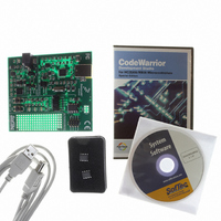
Manufacturer Part Number
DEMO9RS08KA2
Description
DEMO BOARD FOR 9RS08KA2
Manufacturer
Freescale Semiconductor
Series
RS08r
Type
MCUr
Datasheets
1.DEMO9RS08KA2.pdf
(136 pages)
2.DEMO9RS08KA2.pdf
(28 pages)
3.DEMO9RS08KA2.pdf
(2 pages)
4.DEMO9RS08KA2.pdf
(6 pages)
Specifications of DEMO9RS08KA2
Contents
Board, Cable, CD, Documentation, Sample ICs
Processor To Be Evaluated
RS08KA2
Data Bus Width
8 bit
Interface Type
USB
Silicon Manufacturer
Freescale
Core Architecture
RS08
Core Sub-architecture
RS08
Silicon Core Number
MC9RS08
Silicon Family Name
RS08KA
Rohs Compliant
Yes
For Use With/related Products
MC9RS08KA2
Lead Free Status / RoHS Status
Lead free / RoHS Compliant
Available stocks
Company
Part Number
Manufacturer
Quantity
Price
Company:

Part Number:
DEMO9RS08KA2
Manufacturer:
Freescale Semiconductor
Quantity:
135


Appendix A Electrical Characteristics
1
2
3
A.9
This section describes ac timing characteristics for each peripheral system.
A.9.1
1
2
3
118
Stop recovery time (FLL wakeup to previous acquired
frequency)
IREFSTEN=0
IREFSTEN=1
Bus frequency (t
Real time interrupt internal oscillator period
External RESET pulse width
KBI pulse width
KBI pulse width in stop
Port rise and fall time (load = 50 pF)
Data in typical column was characterized at 3.0 V and 5.0 V, 25°C or is typical recommended value.
This parameter is characterized and not tested on each device.
This specification applies to any time the FLL reference source or reference divider is changed, trim value changed or changing
from FLL disabled (FBILP) to FLL enabled (FEI, FBI).
This is the shortest pulse that is guaranteed to pass through the pin input filter circuitry. Shorter pulses may or may not be
recognized.
This is the minimum pulse width that is guaranteed to pass through the pin synchronization circuitry. Shorter pulses may or
may not be recognized. In stop mode, the synchronizer is bypassed so shorter pulses can be recognized in that case.
Timing is shown with respect to 20% V
Slew rate control disabled (PTxSE = 0)
Slew rate control enabled (PTxSE = 1)
AC Characteristics
Control Timing
2
cyc
= 1/f
Characteristic
1
Bus
Parameter
RESET
)
1
Table A-7. Internal Clock Source Specifications
3
DD
MC9RS08KA2 Series Data Sheet, Rev. 4
and 80% V
Table A-8. Control Timing
Figure A-1. Reset Timing
DD
levels. Temperature range –40°C to 85°C.
t_wakeup
t
Symbol
Symbol
t
Rise
t
KBIPWS
t
KBIPW
t
t
t
fll_wu
ir_wu
f
extrst
t
extrst
Bus
RTI
, t
Fall
1.5 t
Min
Min
700
150
100
dc
—
—
—
cyc
Typical
Typ
1000
100
86
11
35
—
—
—
—
1
Freescale Semiconductor
1300
Max
Max
10
—
—
—
—
—
—
MHz
Unit
Unit
μs
μs
ns
ns
ns
ns
Related parts for DEMO9RS08KA2
Image
Part Number
Description
Manufacturer
Datasheet
Request
R

Part Number:
Description:
Manufacturer:
Freescale Semiconductor, Inc
Datasheet:
Part Number:
Description:
Manufacturer:
Freescale Semiconductor, Inc
Datasheet:
Part Number:
Description:
Manufacturer:
Freescale Semiconductor, Inc
Datasheet:
Part Number:
Description:
Manufacturer:
Freescale Semiconductor, Inc
Datasheet:
Part Number:
Description:
Manufacturer:
Freescale Semiconductor, Inc
Datasheet:
Part Number:
Description:
Manufacturer:
Freescale Semiconductor, Inc
Datasheet:
Part Number:
Description:
Manufacturer:
Freescale Semiconductor, Inc
Datasheet:
Part Number:
Description:
Manufacturer:
Freescale Semiconductor, Inc
Datasheet:
Part Number:
Description:
Manufacturer:
Freescale Semiconductor, Inc
Datasheet:
Part Number:
Description:
Manufacturer:
Freescale Semiconductor, Inc
Datasheet:
Part Number:
Description:
Manufacturer:
Freescale Semiconductor, Inc
Datasheet:
Part Number:
Description:
Manufacturer:
Freescale Semiconductor, Inc
Datasheet:
Part Number:
Description:
Manufacturer:
Freescale Semiconductor, Inc
Datasheet:
Part Number:
Description:
Manufacturer:
Freescale Semiconductor, Inc
Datasheet:
Part Number:
Description:
Manufacturer:
Freescale Semiconductor, Inc
Datasheet: