DEMO9RS08KA2 Freescale Semiconductor, DEMO9RS08KA2 Datasheet - Page 30
DEMO9RS08KA2
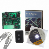
Manufacturer Part Number
DEMO9RS08KA2
Description
DEMO BOARD FOR 9RS08KA2
Manufacturer
Freescale Semiconductor
Series
RS08r
Type
MCUr
Datasheets
1.DEMO9RS08KA2.pdf
(136 pages)
2.DEMO9RS08KA2.pdf
(28 pages)
3.DEMO9RS08KA2.pdf
(2 pages)
4.DEMO9RS08KA2.pdf
(6 pages)
Specifications of DEMO9RS08KA2
Contents
Board, Cable, CD, Documentation, Sample ICs
Processor To Be Evaluated
RS08KA2
Data Bus Width
8 bit
Interface Type
USB
Silicon Manufacturer
Freescale
Core Architecture
RS08
Core Sub-architecture
RS08
Silicon Core Number
MC9RS08
Silicon Family Name
RS08KA
Rohs Compliant
Yes
For Use With/related Products
MC9RS08KA2
Lead Free Status / RoHS Status
Lead free / RoHS Compliant
Available stocks
Company
Part Number
Manufacturer
Quantity
Price
Company:

Part Number:
DEMO9RS08KA2
Manufacturer:
Freescale Semiconductor
Quantity:
135


Chapter 4 Memory
4.6.2
Programming of Flash memory is done on a row basis. A row consists of 64 consecutive bytes starting
from addresses $3X00, $3X40, $3X80, or $3XC0. Use the following procedure to program a row of Flash
memory:
This program sequence is repeated throughout the memory until all data is programmed.
4.6.3
Use the following procedure to mass erase the entire Flash memory:
30
•
•
1. Apply external V
2. Set the PGM bit. This configures the memory for program operation and enables the latching of
3. Write any data to any Flash location, via the high page accessing window $00C0–$00FF, within
4. Wait for a time, t
5. Set the HVEN bit.
6. Wait for a time, t
7. Write data to the Flash location to be programmed.
8. Wait for a time, t
9. Repeat steps 7 and 8 until all bytes within the row are programmed.
10. Clear the PGM bit.
11. Wait for a time, t
12. Clear the HVEN bit.
13. After time, t
14. Remove external V
1. Apply external V
2. Set the MASS bit in the Flash control register.
Up to 1000 program/erase cycles at typical voltage and temperature
Security feature for Flash
address and data for programming.
the address range of the row to be programmed. (Prior to the data writing operation, the PAGESEL
register must be configured correctly to map the high page accessing window to the corresponding
Flash row).
Flash Programming Procedure
Flash Mass Erase Operation
Flash memory cannot be programmed or erased by software code executed
from Flash locations. To program or erase Flash, commands must be
executed from RAM or BDC commands. User code should not enter wait or
stop during erase or program sequence.
These operations must be performed in the order shown; other unrelated
operations may occur between the steps.
rcv
, the memory can be accessed in read mode again.
nvs
pgs
prog
nvh
PP
PP
.
.
PP
.
.
.
.
.
MC9RS08KA2 Series Data Sheet, Rev. 4
NOTE
Freescale Semiconductor
Related parts for DEMO9RS08KA2
Image
Part Number
Description
Manufacturer
Datasheet
Request
R

Part Number:
Description:
Manufacturer:
Freescale Semiconductor, Inc
Datasheet:
Part Number:
Description:
Manufacturer:
Freescale Semiconductor, Inc
Datasheet:
Part Number:
Description:
Manufacturer:
Freescale Semiconductor, Inc
Datasheet:
Part Number:
Description:
Manufacturer:
Freescale Semiconductor, Inc
Datasheet:
Part Number:
Description:
Manufacturer:
Freescale Semiconductor, Inc
Datasheet:
Part Number:
Description:
Manufacturer:
Freescale Semiconductor, Inc
Datasheet:
Part Number:
Description:
Manufacturer:
Freescale Semiconductor, Inc
Datasheet:
Part Number:
Description:
Manufacturer:
Freescale Semiconductor, Inc
Datasheet:
Part Number:
Description:
Manufacturer:
Freescale Semiconductor, Inc
Datasheet:
Part Number:
Description:
Manufacturer:
Freescale Semiconductor, Inc
Datasheet:
Part Number:
Description:
Manufacturer:
Freescale Semiconductor, Inc
Datasheet:
Part Number:
Description:
Manufacturer:
Freescale Semiconductor, Inc
Datasheet:
Part Number:
Description:
Manufacturer:
Freescale Semiconductor, Inc
Datasheet:
Part Number:
Description:
Manufacturer:
Freescale Semiconductor, Inc
Datasheet:
Part Number:
Description:
Manufacturer:
Freescale Semiconductor, Inc
Datasheet: