DEMO9RS08KA2 Freescale Semiconductor, DEMO9RS08KA2 Datasheet - Page 58
DEMO9RS08KA2
Manufacturer Part Number
DEMO9RS08KA2
Description
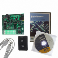
DEMO BOARD FOR 9RS08KA2
Manufacturer
Freescale Semiconductor
Series
RS08r
Type
MCUr
Datasheets
1.DEMO9RS08KA2.pdf
(136 pages)
2.DEMO9RS08KA2.pdf
(28 pages)
3.DEMO9RS08KA2.pdf
(2 pages)
4.DEMO9RS08KA2.pdf
(6 pages)
Specifications of DEMO9RS08KA2
Contents
Board, Cable, CD, Documentation, Sample ICs
Processor To Be Evaluated
RS08KA2
Data Bus Width
8 bit
Interface Type
USB
Silicon Manufacturer
Freescale
Core Architecture
RS08
Core Sub-architecture
RS08
Silicon Core Number
MC9RS08
Silicon Family Name
RS08KA
Rohs Compliant
Yes
For Use With/related Products
MC9RS08KA2
Lead Free Status / RoHS Status
Lead free / RoHS Compliant
Available stocks
Company
Part Number
Manufacturer
Quantity
Price
Company:

Part Number:
DEMO9RS08KA2
Manufacturer:
Freescale Semiconductor
Quantity:
135


Chapter 8 Central Processor Unit (RS08CPUV1)
In addition to the CPU registers, there are three memory mapped registers that are tightly coupled with the
core address generation during data read and write operations. They are the indexed data register (D[X]),
the index register (X), and the page select register (PAGESEL). These registers are located at $000E,
$000F, and $001F, respectively.
8.2.1
This general-purpose 8-bit register is the primary data register for RS08 MCUs. Data can be read from
memory into A with a load accumulator (LDA) instruction. The data in A can be written into memory with
a store accumulator (STA) instruction. Various addressing mode variations allow a great deal of flexibility
in specifying the memory location involved in a load or store instruction. Exchange instructions allow
values to be exchanged between A and SPC high (SHA) and also between A and SPC low (SLA).
Arithmetic, shift, and logical operations can be performed on the value in A as in ADD, SUB, RORA,
INCA, DECA, AND, ORA, EOR, etc. In some of these instructions, such as INCA and LSLA, the value
in A is the only input operand and the result replaces the value in A. In other cases, such as ADD and AND,
there are two operands: the value in A and a second value from memory. The result of the arithmetic or
logical operation replaces the value in A.
Some instructions, such as memory-to-memory move instructions (MOV), do not use the accumulator.
DBNZ also relieves A because it allows a loop counter to be implemented in a memory variable rather than
the accumulator.
During reset, the accumulator is loaded with $00.
58
Accumulator (A)
13
13
INDEXED DATA REGISTER D[X] (location $000E)
7
7
7
SHADOW PROGRAM COUNTER
Figure 8-2. Memory Mapped Registers
CONDITION CODE REGISTER
MC9RS08KA2 Series Data Sheet, Rev. 4
PAGE SELECT REG
PROGRAM COUNTER
INDEX REGISTER
Figure 8-1. CPU Registers
8
7
7
ACCUMULATOR
0
0
0
X (location $000F)
PAGESEL (location $001F)
Z
C
0
0
0
CARRY
ZERO
PC
SPC
CCR
A
Freescale Semiconductor
Related parts for DEMO9RS08KA2
Image
Part Number
Description
Manufacturer
Datasheet
Request
R

Part Number:
Description:
Manufacturer:
Freescale Semiconductor, Inc
Datasheet:
Part Number:
Description:
Manufacturer:
Freescale Semiconductor, Inc
Datasheet:
Part Number:
Description:
Manufacturer:
Freescale Semiconductor, Inc
Datasheet:
Part Number:
Description:
Manufacturer:
Freescale Semiconductor, Inc
Datasheet:
Part Number:
Description:
Manufacturer:
Freescale Semiconductor, Inc
Datasheet:
Part Number:
Description:
Manufacturer:
Freescale Semiconductor, Inc
Datasheet:
Part Number:
Description:
Manufacturer:
Freescale Semiconductor, Inc
Datasheet:
Part Number:
Description:
Manufacturer:
Freescale Semiconductor, Inc
Datasheet:
Part Number:
Description:
Manufacturer:
Freescale Semiconductor, Inc
Datasheet:
Part Number:
Description:
Manufacturer:
Freescale Semiconductor, Inc
Datasheet:
Part Number:
Description:
Manufacturer:
Freescale Semiconductor, Inc
Datasheet:
Part Number:
Description:
Manufacturer:
Freescale Semiconductor, Inc
Datasheet:
Part Number:
Description:
Manufacturer:
Freescale Semiconductor, Inc
Datasheet:
Part Number:
Description:
Manufacturer:
Freescale Semiconductor, Inc
Datasheet:
Part Number:
Description:
Manufacturer:
Freescale Semiconductor, Inc
Datasheet: