DEMO9RS08KA2 Freescale Semiconductor, DEMO9RS08KA2 Datasheet - Page 47
DEMO9RS08KA2
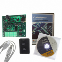
Manufacturer Part Number
DEMO9RS08KA2
Description
DEMO BOARD FOR 9RS08KA2
Manufacturer
Freescale Semiconductor
Series
RS08r
Type
MCUr
Datasheets
1.DEMO9RS08KA2.pdf
(136 pages)
2.DEMO9RS08KA2.pdf
(28 pages)
3.DEMO9RS08KA2.pdf
(2 pages)
4.DEMO9RS08KA2.pdf
(6 pages)
Specifications of DEMO9RS08KA2
Contents
Board, Cable, CD, Documentation, Sample ICs
Processor To Be Evaluated
RS08KA2
Data Bus Width
8 bit
Interface Type
USB
Silicon Manufacturer
Freescale
Core Architecture
RS08
Core Sub-architecture
RS08
Silicon Core Number
MC9RS08
Silicon Family Name
RS08KA
Rohs Compliant
Yes
For Use With/related Products
MC9RS08KA2
Lead Free Status / RoHS Status
Lead free / RoHS Compliant
Available stocks
Company
Part Number
Manufacturer
Quantity
Price
Company:

Part Number:
DEMO9RS08KA2
Manufacturer:
Freescale Semiconductor
Quantity:
135


6.3
This section provides information about the registers associated with the parallel I/O ports that are used
for pin control functions.
Refer to tables in
This section refers to registers and control bits only by their names. A Freescale Semiconductor-provided
equate or header file normally is used to translate these names into the appropriate absolute addresses.
6.3.1
The pins associated with port A are controlled by the registers provided in this section. These registers
control the pin pullup/pulldown and slew rate of the port A pins independent of the parallel I/O registers.
6.3.1.1
An internal pulling device can be enabled for each port pin by setting the corresponding bit in the pulling
device enable register (PTAPEn). The pulling device is disabled if the pin is configured as an output by the
parallel I/O control logic or any shared peripheral output function regardless of the state of the
Freescale Semiconductor
PTADD[5:4,1:0]
PTAD[5:0]
Reset:
Field
5:0
5:4,1:0
Field
W
R
Pin Control Registers
Port A Pin Control Registers
Port A Data Register Bits — For port A pins that are inputs, reads return the logic level on the pin. For port A
pins that are configured as outputs, reads return the last value written to this register. Writes are latched into all
bits of this register. For port A pins that are configured as outputs, the logic level is driven out the corresponding
MCU pin.
Reset forces PTAD to all 0s, but these 0s are not driven out the corresponding pins because reset also configures
all port pins as high-impedance inputs with pullup/pulldowns disabled.
0
Internal Pulling Device Enable
7
0
Data Direction for Port A Bits — These read/write bits control the direction of port A pins and what is read
for PTAD reads.
0 Input (output driver disabled) and reads return the pin value.
1 Output driver enabled for port A bit n and PTAD reads return the contents of PTADn.
Chapter 4,
0
0
6
Figure 6-3. Port A Data Direction Register (PTADD)
“Memory,” for the absolute address assignments of the pin control registers.
Table 6-2. PTADD Register Field Descriptions
Table 6-1. PTAD Register Field Descriptions
PTADD5
MC9RS08KA2 Series Data Sheet, Rev. 4
0
5
PTADD4
0
4
Description
Description
3
0
0
Chapter 6 Parallel Input/Output Control
0
2
0
PTADD1
0
1
PTADD0
0
0
47
Related parts for DEMO9RS08KA2
Image
Part Number
Description
Manufacturer
Datasheet
Request
R

Part Number:
Description:
Manufacturer:
Freescale Semiconductor, Inc
Datasheet:
Part Number:
Description:
Manufacturer:
Freescale Semiconductor, Inc
Datasheet:
Part Number:
Description:
Manufacturer:
Freescale Semiconductor, Inc
Datasheet:
Part Number:
Description:
Manufacturer:
Freescale Semiconductor, Inc
Datasheet:
Part Number:
Description:
Manufacturer:
Freescale Semiconductor, Inc
Datasheet:
Part Number:
Description:
Manufacturer:
Freescale Semiconductor, Inc
Datasheet:
Part Number:
Description:
Manufacturer:
Freescale Semiconductor, Inc
Datasheet:
Part Number:
Description:
Manufacturer:
Freescale Semiconductor, Inc
Datasheet:
Part Number:
Description:
Manufacturer:
Freescale Semiconductor, Inc
Datasheet:
Part Number:
Description:
Manufacturer:
Freescale Semiconductor, Inc
Datasheet:
Part Number:
Description:
Manufacturer:
Freescale Semiconductor, Inc
Datasheet:
Part Number:
Description:
Manufacturer:
Freescale Semiconductor, Inc
Datasheet:
Part Number:
Description:
Manufacturer:
Freescale Semiconductor, Inc
Datasheet:
Part Number:
Description:
Manufacturer:
Freescale Semiconductor, Inc
Datasheet:
Part Number:
Description:
Manufacturer:
Freescale Semiconductor, Inc
Datasheet: