DEMO9RS08KA2 Freescale Semiconductor, DEMO9RS08KA2 Datasheet - Page 33
DEMO9RS08KA2
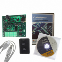
Manufacturer Part Number
DEMO9RS08KA2
Description
DEMO BOARD FOR 9RS08KA2
Manufacturer
Freescale Semiconductor
Series
RS08r
Type
MCUr
Datasheets
1.DEMO9RS08KA2.pdf
(136 pages)
2.DEMO9RS08KA2.pdf
(28 pages)
3.DEMO9RS08KA2.pdf
(2 pages)
4.DEMO9RS08KA2.pdf
(6 pages)
Specifications of DEMO9RS08KA2
Contents
Board, Cable, CD, Documentation, Sample ICs
Processor To Be Evaluated
RS08KA2
Data Bus Width
8 bit
Interface Type
USB
Silicon Manufacturer
Freescale
Core Architecture
RS08
Core Sub-architecture
RS08
Silicon Core Number
MC9RS08
Silicon Family Name
RS08KA
Rohs Compliant
Yes
For Use With/related Products
MC9RS08KA2
Lead Free Status / RoHS Status
Lead free / RoHS Compliant
Available stocks
Company
Part Number
Manufacturer
Quantity
Price
Company:

Part Number:
DEMO9RS08KA2
Manufacturer:
Freescale Semiconductor
Quantity:
135


4.7.2
1
4.8
There is a 64-byte window ($00C0–$00FF) in the direct-page reserved for paging access. Programming
the page select register determines the corresponding 64-byte block on the memory map for direct-page
access. For example, when the PAGESEL register is programmed with value $08, the high page registers
($0200–$023F) can be accessed through the paging window ($00C0–$00FF) via direct addressing mode
instructions.
Freescale Semiconductor
When Flash security is engaged, writing to PGM bit has no effect. As a result, Flash programming is not allowed.
AD[13:6]
HVEN
MASS
PGM
Field
Field
7:0
3
2
0
Reset
Reset
1
W
W
Page Select Register (PAGESEL)
R
R
Flash Control Register (FLCR)
High Voltage Enable — This read/write bit enables high voltages to the Flash array for program and erase
operations. HVEN can be set only if either PGM = 1 or MASS = 1 and the proper sequence for program or erase
is followed.
0 High voltage disabled to array.
1 High voltage enabled to array.
Mass Erase Control Bit — This read/write bit configures the memory for mass erase operation.
0 Mass erase operation not selected.
1 Mass erase operation selected.
Program Control Bit — This read/write bit configures the memory for program operation. PGM is interlocked
with the MASS bit such that both bits cannot be equal to 1 or set to 1 at the same time.
0 Program operation not selected.
1 Program operation selected.
Page Selector— These bits define the address line bit 6 to bit 13, which determines the 64-byte block boundary
of the memory block accessed via the direct page window. See
AD13
0
0
0
7
7
= Unimplemented or Reserved
AD12
6
0
0
6
0
Figure 4-5. Page Select Register (PAGESEL)
Figure 4-4. Flash Control Register (FLCR)
Table 4-4. PAGESEL Field Descriptions
MC9RS08KA2 Series Data Sheet, Rev. 4
Table 4-3. FLCR Field Descriptions
AD11
0
0
0
5
5
AD10
4
0
0
4
0
Description
Description
HVEN
AD9
0
1
3
3
Figure 4-6
MASS
AD8
and
2
0
2
0
Table
4-5.
AD7
0
0
0
1
1
Chapter 4 Memory
PGM
AD6
0
0
0
0
1
33
Related parts for DEMO9RS08KA2
Image
Part Number
Description
Manufacturer
Datasheet
Request
R

Part Number:
Description:
Manufacturer:
Freescale Semiconductor, Inc
Datasheet:
Part Number:
Description:
Manufacturer:
Freescale Semiconductor, Inc
Datasheet:
Part Number:
Description:
Manufacturer:
Freescale Semiconductor, Inc
Datasheet:
Part Number:
Description:
Manufacturer:
Freescale Semiconductor, Inc
Datasheet:
Part Number:
Description:
Manufacturer:
Freescale Semiconductor, Inc
Datasheet:
Part Number:
Description:
Manufacturer:
Freescale Semiconductor, Inc
Datasheet:
Part Number:
Description:
Manufacturer:
Freescale Semiconductor, Inc
Datasheet:
Part Number:
Description:
Manufacturer:
Freescale Semiconductor, Inc
Datasheet:
Part Number:
Description:
Manufacturer:
Freescale Semiconductor, Inc
Datasheet:
Part Number:
Description:
Manufacturer:
Freescale Semiconductor, Inc
Datasheet:
Part Number:
Description:
Manufacturer:
Freescale Semiconductor, Inc
Datasheet:
Part Number:
Description:
Manufacturer:
Freescale Semiconductor, Inc
Datasheet:
Part Number:
Description:
Manufacturer:
Freescale Semiconductor, Inc
Datasheet:
Part Number:
Description:
Manufacturer:
Freescale Semiconductor, Inc
Datasheet:
Part Number:
Description:
Manufacturer:
Freescale Semiconductor, Inc
Datasheet: