DEMO9RS08KA2 Freescale Semiconductor, DEMO9RS08KA2 Datasheet - Page 45
DEMO9RS08KA2
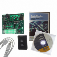
Manufacturer Part Number
DEMO9RS08KA2
Description
DEMO BOARD FOR 9RS08KA2
Manufacturer
Freescale Semiconductor
Series
RS08r
Type
MCUr
Datasheets
1.DEMO9RS08KA2.pdf
(136 pages)
2.DEMO9RS08KA2.pdf
(28 pages)
3.DEMO9RS08KA2.pdf
(2 pages)
4.DEMO9RS08KA2.pdf
(6 pages)
Specifications of DEMO9RS08KA2
Contents
Board, Cable, CD, Documentation, Sample ICs
Processor To Be Evaluated
RS08KA2
Data Bus Width
8 bit
Interface Type
USB
Silicon Manufacturer
Freescale
Core Architecture
RS08
Core Sub-architecture
RS08
Silicon Core Number
MC9RS08
Silicon Family Name
RS08KA
Rohs Compliant
Yes
For Use With/related Products
MC9RS08KA2
Lead Free Status / RoHS Status
Lead free / RoHS Compliant
Available stocks
Company
Part Number
Manufacturer
Quantity
Price
Company:

Part Number:
DEMO9RS08KA2
Manufacturer:
Freescale Semiconductor
Quantity:
135


Chapter 6
Parallel Input/Output Control
This section explains software controls related to parallel input/output (I/O) and pin control. The
MC9RS08KA2 Series has one parallel I/O port, which includes two I/O pins in the 6-pin package or four
I/O pins in the 8-pin packages, one output-only pin, and one input-only pin. See
Connections,” for more information about pin assignments and external hardware considerations for these
pins.
All of these I/O pins are shared with on-chip peripheral functions as shown in
modules have priority over the I/Os so that when a peripheral is enabled, the I/O functions associated with
the shared pins are disabled. After reset, the shared peripheral functions are disabled so that the pins are
controlled by the I/O. All of the I/Os are configured as inputs (PTADDn = 0) with pullup/pulldown devices
disabled (PTAPEn = 0), except for output-only pin PTA3, which defaults to the BKGD/MS function.
Reading and writing of parallel I/Os is performed through the port data registers. The direction, either input
or output, is controlled through the port data direction registers. The parallel I/O port function for an
individual pin is illustrated in the block diagram shown in
The data direction control bit (PTADDn) determines whether the output buffer for the associated pin is
enabled, and also controls the source for port data register reads. The input buffer for the associated pin is
always enabled unless the pin is enabled as an analog function or is an output-only pin.
Freescale Semiconductor
Port Read
BUSCLK
Data
Figure 6-1. Parallel I/O Block Diagram
MC9RS08KA2 Series Data Sheet, Rev. 4
PTADDn
D
D
PTADn
Q
Q
1
0
Figure
6-1.
Synchronizer
Table
Chapter 2, “Pins and
Output Enable
Output Data
2-1. The peripheral
Input Data
45
Related parts for DEMO9RS08KA2
Image
Part Number
Description
Manufacturer
Datasheet
Request
R

Part Number:
Description:
Manufacturer:
Freescale Semiconductor, Inc
Datasheet:
Part Number:
Description:
Manufacturer:
Freescale Semiconductor, Inc
Datasheet:
Part Number:
Description:
Manufacturer:
Freescale Semiconductor, Inc
Datasheet:
Part Number:
Description:
Manufacturer:
Freescale Semiconductor, Inc
Datasheet:
Part Number:
Description:
Manufacturer:
Freescale Semiconductor, Inc
Datasheet:
Part Number:
Description:
Manufacturer:
Freescale Semiconductor, Inc
Datasheet:
Part Number:
Description:
Manufacturer:
Freescale Semiconductor, Inc
Datasheet:
Part Number:
Description:
Manufacturer:
Freescale Semiconductor, Inc
Datasheet:
Part Number:
Description:
Manufacturer:
Freescale Semiconductor, Inc
Datasheet:
Part Number:
Description:
Manufacturer:
Freescale Semiconductor, Inc
Datasheet:
Part Number:
Description:
Manufacturer:
Freescale Semiconductor, Inc
Datasheet:
Part Number:
Description:
Manufacturer:
Freescale Semiconductor, Inc
Datasheet:
Part Number:
Description:
Manufacturer:
Freescale Semiconductor, Inc
Datasheet:
Part Number:
Description:
Manufacturer:
Freescale Semiconductor, Inc
Datasheet:
Part Number:
Description:
Manufacturer:
Freescale Semiconductor, Inc
Datasheet: