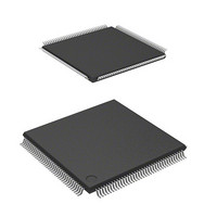
HD64F2166VTE33 Renesas Electronics America, HD64F2166VTE33 Datasheet - Page 297

HD64F2166VTE33
Manufacturer Part Number
HD64F2166VTE33
Description
IC H8S MCU FLASH 512K 144-TQFP
Manufacturer
Renesas Electronics America
Series
H8® H8S/2100r
Specifications of HD64F2166VTE33
Core Processor
H8S/2000
Core Size
16-Bit
Speed
33MHz
Connectivity
I²C, IrDA, LPC, SCI, SmartCard
Peripherals
POR, PWM, WDT
Number Of I /o
106
Program Memory Size
512KB (512K x 8)
Program Memory Type
FLASH
Ram Size
40K x 8
Voltage - Supply (vcc/vdd)
3 V ~ 3.6 V
Data Converters
A/D 8x10b; D/A 2x8b
Oscillator Type
Internal
Operating Temperature
-20°C ~ 75°C
Package / Case
144-TQFP, 144-VQFP
Lead Free Status / RoHS Status
Contains lead / RoHS non-compliant
Eeprom Size
-
Available stocks
Company
Part Number
Manufacturer
Quantity
Price
Company:
Part Number:
HD64F2166VTE33V
Manufacturer:
Renesas
Quantity:
200
Company:
Part Number:
HD64F2166VTE33V
Manufacturer:
ON
Quantity:
75
Part Number:
HD64F2166VTE33V
Manufacturer:
RENESAS/瑞萨
Quantity:
20 000
- Current page: 297 of 876
- Download datasheet (5Mb)
Table 9.3
9.3.2
PWDR are 8-bit readable/writable registers. The PWM has sixteen PWM data registers. Each
PWDR specifies the duty cycle of the basic pulse to be output, and the number of additional
pulses. The value set in PWDR corresponds to a 0 or 1 ratio in the conversion period. The upper
four bits specify the duty cycle of the basic pulse as 0/16 to 15/16 with a resolution of 1/16. The
lower four bits specify how many extra pulses are to be added within the conversion period
comprising 16 basic pulses. Thus, a specification of 0/256 to 255/256 is possible for 0/1 ratios
within the conversion period. For 256/256 (100%) output, port output should be used.
9.3.3
Each PWDPR selects the PWM output phase.
• PWDPRA
Internal Clock
Frequency
φ
φ/2
φ/4
φ/8
φ/16
Bit
7 to 0 OS7 to OS0 All 0
Bit Name
PWM Data Registers 15 to 0 (PWDR15 to PWDR0)
PWM Data Polarity Registers A and B (PWDPRA and PWDPRB)
Resolution, PWM Conversion Period, and Carrier Frequency when φ = 33 MHz
Initial
Value R/W Description
Resolution
30 ns
61 ns
121 ns
242 ns
485 ns
R/W Output Select 7 to 0
These bits select the PWM output phase. Bits OS7 to OS0
correspond to outputs PW7 to PW0.
0: PWM direct output (PWDR value corresponds to high width
1: PWM inverted output (PWDR value corresponds to low
of output)
width of output)
PWM Conversion
Period
7.76 µs
15.52 µs
31.03 µs
62.06 µs
124.12 µs
Rev. 3.00, 03/04, page 255 of 830
Carrier Frequency
2063 kHz
1031 kHz
515.6 kHz
257.8 kHz
128.9 kHz
Related parts for HD64F2166VTE33
Image
Part Number
Description
Manufacturer
Datasheet
Request
R

Part Number:
Description:
KIT STARTER FOR M16C/29
Manufacturer:
Renesas Electronics America
Datasheet:

Part Number:
Description:
KIT STARTER FOR R8C/2D
Manufacturer:
Renesas Electronics America
Datasheet:

Part Number:
Description:
R0K33062P STARTER KIT
Manufacturer:
Renesas Electronics America
Datasheet:

Part Number:
Description:
KIT STARTER FOR R8C/23 E8A
Manufacturer:
Renesas Electronics America
Datasheet:

Part Number:
Description:
KIT STARTER FOR R8C/25
Manufacturer:
Renesas Electronics America
Datasheet:

Part Number:
Description:
KIT STARTER H8S2456 SHARPE DSPLY
Manufacturer:
Renesas Electronics America
Datasheet:

Part Number:
Description:
KIT STARTER FOR R8C38C
Manufacturer:
Renesas Electronics America
Datasheet:

Part Number:
Description:
KIT STARTER FOR R8C35C
Manufacturer:
Renesas Electronics America
Datasheet:

Part Number:
Description:
KIT STARTER FOR R8CL3AC+LCD APPS
Manufacturer:
Renesas Electronics America
Datasheet:

Part Number:
Description:
KIT STARTER FOR RX610
Manufacturer:
Renesas Electronics America
Datasheet:

Part Number:
Description:
KIT STARTER FOR R32C/118
Manufacturer:
Renesas Electronics America
Datasheet:

Part Number:
Description:
KIT DEV RSK-R8C/26-29
Manufacturer:
Renesas Electronics America
Datasheet:

Part Number:
Description:
KIT STARTER FOR SH7124
Manufacturer:
Renesas Electronics America
Datasheet:

Part Number:
Description:
KIT STARTER FOR H8SX/1622
Manufacturer:
Renesas Electronics America
Datasheet:

Part Number:
Description:
KIT DEV FOR SH7203
Manufacturer:
Renesas Electronics America
Datasheet:


