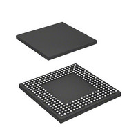
D17760BP200ADV Renesas Electronics America, D17760BP200ADV Datasheet - Page 1130

D17760BP200ADV
Manufacturer Part Number
D17760BP200ADV
Description
MPU 3V 8K,PB-FREE, 256-BGA
Manufacturer
Renesas Electronics America
Series
SuperH® SH7750r
Datasheet
1.D6417760BP200ADV.pdf
(1418 pages)
Specifications of D17760BP200ADV
Core Processor
SH-4
Core Size
32-Bit
Speed
200MHz
Connectivity
Audio Codec, CAN, EBI/EMI, FIFO, I²C, MFI, MMC, SCI, Serial Sound, SIM, SPI, USB
Peripherals
DMA, LCD, POR, WDT
Number Of I /o
69
Program Memory Type
ROMless
Ram Size
48K x 8
Voltage - Supply (vcc/vdd)
1.4 V ~ 1.6 V
Data Converters
A/D 4x10b
Oscillator Type
Internal
Operating Temperature
-40°C ~ 85°C
Package / Case
256-BGA
Lead Free Status / RoHS Status
Lead free / RoHS Compliant
Eeprom Size
-
Program Memory Size
-
Available stocks
Company
Part Number
Manufacturer
Quantity
Price
Company:
Part Number:
D17760BP200ADV
Manufacturer:
Renesas Electronics America
Quantity:
10 000
- Current page: 1130 of 1418
- Download datasheet (9Mb)
Rev. 2.00 Feb. 12, 2010 Page 1046 of 1330
REJ09B0554-0200
Bit
11
10
9, 8
7
6
5
4
3, 2
Bit
Name
TRGE1
TRGE0
⎯
CKSL1
CKSL0
MDS1
MDS0
⎯
Initial
Value
0
0
All 0
0
1
0
0
All 0
R/W
R/W
R/W
R
R/W
R/W
R/W
R/W
R
Description
Trigger Enable
External trigger input permits or prohibits A/D conversion.
These bits must be set while conversion is stopped.
00: When an external trigger is input, A/D conversion
01: Setting prohibited
10: Setting prohibited
11: A/D conversion starts at the falling edge of an input
Note: Clear bits TRGE1 and TRGE0 to 0 before
Reserved
These bits are always read as 0, and the write value
should always be 0.
Clock Select
These bits select the A/D conversion clock division ratio.
00: Pck/4
01: Pck/8
10: Pck/16
11: Pck/32
Note: For the Pck and clock division ratio settings, refer
Conversion Mode Select
These bits select single mode, multi mode, or scan mode.
For details on modes, see section 29.4, Operation.
The combination of MDS1 = 0 and MDS0 = 1 should not
be selected.
00: Single mode
01: Setting prohibited
10: Multi mode
11: Scan mode
Reserved
These bits are always read as 0, and the write value
should always be 0.
does not start
signal from the external trigger input pin (ADTRG)
(except in multi mode)
switching the trigger signal.
to section 29.7.3, Pck and Clock Division Ratio
Settings.
Related parts for D17760BP200ADV
Image
Part Number
Description
Manufacturer
Datasheet
Request
R

Part Number:
Description:
KIT STARTER FOR M16C/29
Manufacturer:
Renesas Electronics America
Datasheet:

Part Number:
Description:
KIT STARTER FOR R8C/2D
Manufacturer:
Renesas Electronics America
Datasheet:

Part Number:
Description:
R0K33062P STARTER KIT
Manufacturer:
Renesas Electronics America
Datasheet:

Part Number:
Description:
KIT STARTER FOR R8C/23 E8A
Manufacturer:
Renesas Electronics America
Datasheet:

Part Number:
Description:
KIT STARTER FOR R8C/25
Manufacturer:
Renesas Electronics America
Datasheet:

Part Number:
Description:
KIT STARTER H8S2456 SHARPE DSPLY
Manufacturer:
Renesas Electronics America
Datasheet:

Part Number:
Description:
KIT STARTER FOR R8C38C
Manufacturer:
Renesas Electronics America
Datasheet:

Part Number:
Description:
KIT STARTER FOR R8C35C
Manufacturer:
Renesas Electronics America
Datasheet:

Part Number:
Description:
KIT STARTER FOR R8CL3AC+LCD APPS
Manufacturer:
Renesas Electronics America
Datasheet:

Part Number:
Description:
KIT STARTER FOR RX610
Manufacturer:
Renesas Electronics America
Datasheet:

Part Number:
Description:
KIT STARTER FOR R32C/118
Manufacturer:
Renesas Electronics America
Datasheet:

Part Number:
Description:
KIT DEV RSK-R8C/26-29
Manufacturer:
Renesas Electronics America
Datasheet:

Part Number:
Description:
KIT STARTER FOR SH7124
Manufacturer:
Renesas Electronics America
Datasheet:

Part Number:
Description:
KIT STARTER FOR H8SX/1622
Manufacturer:
Renesas Electronics America
Datasheet:

Part Number:
Description:
KIT DEV FOR SH7203
Manufacturer:
Renesas Electronics America
Datasheet:


