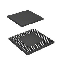
D17760BP200ADV Renesas Electronics America, D17760BP200ADV Datasheet - Page 245

D17760BP200ADV
Manufacturer Part Number
D17760BP200ADV
Description
MPU 3V 8K,PB-FREE, 256-BGA
Manufacturer
Renesas Electronics America
Series
SuperH® SH7750r
Datasheet
1.D6417760BP200ADV.pdf
(1418 pages)
Specifications of D17760BP200ADV
Core Processor
SH-4
Core Size
32-Bit
Speed
200MHz
Connectivity
Audio Codec, CAN, EBI/EMI, FIFO, I²C, MFI, MMC, SCI, Serial Sound, SIM, SPI, USB
Peripherals
DMA, LCD, POR, WDT
Number Of I /o
69
Program Memory Type
ROMless
Ram Size
48K x 8
Voltage - Supply (vcc/vdd)
1.4 V ~ 1.6 V
Data Converters
A/D 4x10b
Oscillator Type
Internal
Operating Temperature
-40°C ~ 85°C
Package / Case
256-BGA
Lead Free Status / RoHS Status
Lead free / RoHS Compliant
Eeprom Size
-
Program Memory Size
-
Available stocks
Company
Part Number
Manufacturer
Quantity
Price
Company:
Part Number:
D17760BP200ADV
Manufacturer:
Renesas Electronics America
Quantity:
10 000
- Current page: 245 of 1418
- Download datasheet (9Mb)
3. Cache hit (copy-back)
4. Cache hit (write-through)
5. Cache miss (no copy-back/write-back)
6. Cache miss (write-through)
7. Cache miss (with copy-back/write-back)
A data write in accordance with the access size (quadword/longword/word/byte) is performed
for the data indexed by effective address bits [4:0] of the data field of the cache line indexed by
effective address bits [13:5]. Then 1 is written to the U bit.
A data write in accordance with the access size (quadword/longword/word/byte) is performed
for the data indexed by effective address bits [4:0] of the data field of the cache line indexed by
effective address bits [13:5]. A write is also performed to the corresponding external memory
using the specified access size.
A data write in accordance with the access size (quadword/longword/word/byte) is performed
for the data indexed by effective address bits [4:0] of the data field of the cache line indexed by
effective address bits [13:5]. Then, data is read into the cache line from the external memory
space corresponding to the effective address. Data reading is performed, using the wraparound
method, in order from the longword data corresponding to the effective address, and one cache
line of data is read excluding the written data. During this time, the CPU can execute the next
processing. When reading of one line of data is completed, the tag corresponding to the
effective address is recorded in the cache, and 1 is written to the V bit and U bit.
A write of the specified access size is performed to the external memory corresponding to the
effective address. In this case, a write to cache is not performed.
The tag and data field of the cache line indexed by effective address bits [13:5] are first saved
in the write-back buffer, and then a data write in accordance with the access size
(quadword/longword/word/byte) is performed for the data indexed by effective address bits
[4:0] of the data field of the cache line indexed by effective address bits [13:5]. Then, data is
read into the cache line from the external memory space corresponding to the effective
address. Data reading is performed, using the wraparound method, in order from the longword
data corresponding to the effective address, and one cache line of data is read excluding the
written data. During this time, the CPU can execute the next processing. When reading of one
line of data is completed, the tag corresponding to the effective address is recorded in the
cache, and 1 is written to the V bit and U bit. The data in the write-back buffer is then written
back to external memory.
Rev. 2.00 Feb. 12, 2010 Page 161 of 1330
REJ09B0554-0200
Related parts for D17760BP200ADV
Image
Part Number
Description
Manufacturer
Datasheet
Request
R

Part Number:
Description:
KIT STARTER FOR M16C/29
Manufacturer:
Renesas Electronics America
Datasheet:

Part Number:
Description:
KIT STARTER FOR R8C/2D
Manufacturer:
Renesas Electronics America
Datasheet:

Part Number:
Description:
R0K33062P STARTER KIT
Manufacturer:
Renesas Electronics America
Datasheet:

Part Number:
Description:
KIT STARTER FOR R8C/23 E8A
Manufacturer:
Renesas Electronics America
Datasheet:

Part Number:
Description:
KIT STARTER FOR R8C/25
Manufacturer:
Renesas Electronics America
Datasheet:

Part Number:
Description:
KIT STARTER H8S2456 SHARPE DSPLY
Manufacturer:
Renesas Electronics America
Datasheet:

Part Number:
Description:
KIT STARTER FOR R8C38C
Manufacturer:
Renesas Electronics America
Datasheet:

Part Number:
Description:
KIT STARTER FOR R8C35C
Manufacturer:
Renesas Electronics America
Datasheet:

Part Number:
Description:
KIT STARTER FOR R8CL3AC+LCD APPS
Manufacturer:
Renesas Electronics America
Datasheet:

Part Number:
Description:
KIT STARTER FOR RX610
Manufacturer:
Renesas Electronics America
Datasheet:

Part Number:
Description:
KIT STARTER FOR R32C/118
Manufacturer:
Renesas Electronics America
Datasheet:

Part Number:
Description:
KIT DEV RSK-R8C/26-29
Manufacturer:
Renesas Electronics America
Datasheet:

Part Number:
Description:
KIT STARTER FOR SH7124
Manufacturer:
Renesas Electronics America
Datasheet:

Part Number:
Description:
KIT STARTER FOR H8SX/1622
Manufacturer:
Renesas Electronics America
Datasheet:

Part Number:
Description:
KIT DEV FOR SH7203
Manufacturer:
Renesas Electronics America
Datasheet:


