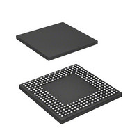
D17760BP200ADV Renesas Electronics America, D17760BP200ADV Datasheet - Page 366

D17760BP200ADV
Manufacturer Part Number
D17760BP200ADV
Description
MPU 3V 8K,PB-FREE, 256-BGA
Manufacturer
Renesas Electronics America
Series
SuperH® SH7750r
Datasheet
1.D6417760BP200ADV.pdf
(1418 pages)
Specifications of D17760BP200ADV
Core Processor
SH-4
Core Size
32-Bit
Speed
200MHz
Connectivity
Audio Codec, CAN, EBI/EMI, FIFO, I²C, MFI, MMC, SCI, Serial Sound, SIM, SPI, USB
Peripherals
DMA, LCD, POR, WDT
Number Of I /o
69
Program Memory Type
ROMless
Ram Size
48K x 8
Voltage - Supply (vcc/vdd)
1.4 V ~ 1.6 V
Data Converters
A/D 4x10b
Oscillator Type
Internal
Operating Temperature
-40°C ~ 85°C
Package / Case
256-BGA
Lead Free Status / RoHS Status
Lead free / RoHS Compliant
Eeprom Size
-
Program Memory Size
-
Available stocks
Company
Part Number
Manufacturer
Quantity
Price
Company:
Part Number:
D17760BP200ADV
Manufacturer:
Renesas Electronics America
Quantity:
10 000
- Current page: 366 of 1418
- Download datasheet (9Mb)
Notes: n = 0 to 6; m = 1 and 4
10.5.8
WCR4 is a 32-bit readable/writable register that specifies the negation period for the CS1 signal.
Specifying bits CSH1 and CSH0 can insert the negation cycles from 0 to 3. If the CS1 negate
period is set, it must be set to match the WCR3 data hold time (A1H[1:0]). If the CS1 negate
period is not specified (CSH[1:0] = 00), there is no need to match the WCR3 data hold time
(A1H[1:0]).
Initial value:
Initial value:
Rev. 2.00 Feb. 12, 2010 Page 282 of 1330
REJ09B0554-0200
Bit
4n + 1
4n
4m + 3 AmRDH
R/W:
R/W:
Bit:
Bit:
* For area 1, only use the combinations listed in table 10.9 for the settings.
Bit
Name
AnH1*
AnH0*
Wait Control Register 4 (WCR4)
31
15
R
R
0
0
-
-
30
14
R
R
0
0
-
-
Initial
Value
All 1
All 1
All 0
29
13
R
R
0
0
-
-
28
12
R
R
0
0
-
-
R/W
R/W
R/W
R/W
27
11
R
R
0
0
-
-
26
10
R
R
0
0
-
-
Description
Area n Data Hold Time
For writing, specifies the number of cycles to be inserted
during the data hold time after the write strobe is
negated. For reading, specifies the number of cycles to
be inserted during the data hold time after the data
sampling timing. Valid only for SRAM interface, byte
control SRAM interface, and burst ROM interface:
00:
01:
10:
11:
Read-Strobe Negate Timing
For reading, these bits specify the timing for the negation
of read strobe. These bits should be cleared to 0 when
byte control SRAM interface is in use.
See figure 10.12.
25
R
R
0
9
0
-
-
Cycles to be inserted during the data hold time
0
1
2
3
24
R
R
0
8
0
-
-
23
R
R
0
7
0
-
-
22
R
R
0
0
6
-
-
21
R
R
0
5
-
0
-
20
R
R
0
4
-
0
-
19
R
R
-
0
3
-
0
18
R
R
0
2
0
-
-
CSH1 CSH0
R/W
17
R
-
0
1
0
R/W
16
R
0
0
0
-
Related parts for D17760BP200ADV
Image
Part Number
Description
Manufacturer
Datasheet
Request
R

Part Number:
Description:
KIT STARTER FOR M16C/29
Manufacturer:
Renesas Electronics America
Datasheet:

Part Number:
Description:
KIT STARTER FOR R8C/2D
Manufacturer:
Renesas Electronics America
Datasheet:

Part Number:
Description:
R0K33062P STARTER KIT
Manufacturer:
Renesas Electronics America
Datasheet:

Part Number:
Description:
KIT STARTER FOR R8C/23 E8A
Manufacturer:
Renesas Electronics America
Datasheet:

Part Number:
Description:
KIT STARTER FOR R8C/25
Manufacturer:
Renesas Electronics America
Datasheet:

Part Number:
Description:
KIT STARTER H8S2456 SHARPE DSPLY
Manufacturer:
Renesas Electronics America
Datasheet:

Part Number:
Description:
KIT STARTER FOR R8C38C
Manufacturer:
Renesas Electronics America
Datasheet:

Part Number:
Description:
KIT STARTER FOR R8C35C
Manufacturer:
Renesas Electronics America
Datasheet:

Part Number:
Description:
KIT STARTER FOR R8CL3AC+LCD APPS
Manufacturer:
Renesas Electronics America
Datasheet:

Part Number:
Description:
KIT STARTER FOR RX610
Manufacturer:
Renesas Electronics America
Datasheet:

Part Number:
Description:
KIT STARTER FOR R32C/118
Manufacturer:
Renesas Electronics America
Datasheet:

Part Number:
Description:
KIT DEV RSK-R8C/26-29
Manufacturer:
Renesas Electronics America
Datasheet:

Part Number:
Description:
KIT STARTER FOR SH7124
Manufacturer:
Renesas Electronics America
Datasheet:

Part Number:
Description:
KIT STARTER FOR H8SX/1622
Manufacturer:
Renesas Electronics America
Datasheet:

Part Number:
Description:
KIT DEV FOR SH7203
Manufacturer:
Renesas Electronics America
Datasheet:


