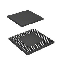
D17760BP200ADV Renesas Electronics America, D17760BP200ADV Datasheet - Page 772

D17760BP200ADV
Manufacturer Part Number
D17760BP200ADV
Description
MPU 3V 8K,PB-FREE, 256-BGA
Manufacturer
Renesas Electronics America
Series
SuperH® SH7750r
Datasheet
1.D6417760BP200ADV.pdf
(1418 pages)
Specifications of D17760BP200ADV
Core Processor
SH-4
Core Size
32-Bit
Speed
200MHz
Connectivity
Audio Codec, CAN, EBI/EMI, FIFO, I²C, MFI, MMC, SCI, Serial Sound, SIM, SPI, USB
Peripherals
DMA, LCD, POR, WDT
Number Of I /o
69
Program Memory Type
ROMless
Ram Size
48K x 8
Voltage - Supply (vcc/vdd)
1.4 V ~ 1.6 V
Data Converters
A/D 4x10b
Oscillator Type
Internal
Operating Temperature
-40°C ~ 85°C
Package / Case
256-BGA
Lead Free Status / RoHS Status
Lead free / RoHS Compliant
Eeprom Size
-
Program Memory Size
-
Available stocks
Company
Part Number
Manufacturer
Quantity
Price
Company:
Part Number:
D17760BP200ADV
Manufacturer:
Renesas Electronics America
Quantity:
10 000
- Current page: 772 of 1418
- Download datasheet (9Mb)
Section 19 I
19.4
19.4.1
These blocks filter out glitches on signals coming from the I
to one clock cycle is rejected. (See the description of the clock control register for details of
internal clock). This is specified for the faster I
slower I
These blocks also perform resynchronization of bus signals to the internal clock.
19.4.2
The clock generator has two functions. Firstly, it generates the SCL I
of the master or slave interface. Secondly, it controls the internal clock rate, used by filtering
blocks and the master and slave interfaces. This operates as a clock-enable signal to the registers
in the filter, master, and slave interfaces.
19.4.3
Master and slave interfaces run independently and in parallel. The master interface controls the
transmission of address and data on the I
part in transmissions if its programmed address is seen on the bus. Both interfaces communicate
with the control register and the status registers independently. Only one interrupt line comes from
the I
19.4.4
To make software interface to the I
statuses are interlocked in the master and slave interface operations. The status bits involved are
described below.
(1) MDR and SDR (Single Buffer Mode)
MDR and SDR are set to 1 when data is received. Clear these bits to 0 after reading the receive
data register. If data is received while MDR and SDR are 1, hardware recognizes that unread data
remains in the receive data register, automatically holds SCL at low level and suspends data
transfer. In this case, clearing these bits to 0 after reading the receive data will resume transfer.
When receiving data consecutively, be sure to clear MDR and SDR to 0 after reading the receive
data register.
Rev. 2.00 Feb. 12, 2010 Page 688 of 1330
REJ09B0554-0200
2
C bus interface module; the source could be either the master or the slave.
2
C bus rate specification.
Operation
Data and Clock Filters
Clock Generator
Master and Slave Interfaces
Software Status Interlocking
2
C Bus Interface
2
C bus interface module as robust and simple as possible, some
2
C bus. The slave interface monitors the I
2
C bus rate (400 kHz) but does not violate the
2
C bus. A glitch with a duration of up
2
C bus clock under command
2
C bus and takes
Related parts for D17760BP200ADV
Image
Part Number
Description
Manufacturer
Datasheet
Request
R

Part Number:
Description:
KIT STARTER FOR M16C/29
Manufacturer:
Renesas Electronics America
Datasheet:

Part Number:
Description:
KIT STARTER FOR R8C/2D
Manufacturer:
Renesas Electronics America
Datasheet:

Part Number:
Description:
R0K33062P STARTER KIT
Manufacturer:
Renesas Electronics America
Datasheet:

Part Number:
Description:
KIT STARTER FOR R8C/23 E8A
Manufacturer:
Renesas Electronics America
Datasheet:

Part Number:
Description:
KIT STARTER FOR R8C/25
Manufacturer:
Renesas Electronics America
Datasheet:

Part Number:
Description:
KIT STARTER H8S2456 SHARPE DSPLY
Manufacturer:
Renesas Electronics America
Datasheet:

Part Number:
Description:
KIT STARTER FOR R8C38C
Manufacturer:
Renesas Electronics America
Datasheet:

Part Number:
Description:
KIT STARTER FOR R8C35C
Manufacturer:
Renesas Electronics America
Datasheet:

Part Number:
Description:
KIT STARTER FOR R8CL3AC+LCD APPS
Manufacturer:
Renesas Electronics America
Datasheet:

Part Number:
Description:
KIT STARTER FOR RX610
Manufacturer:
Renesas Electronics America
Datasheet:

Part Number:
Description:
KIT STARTER FOR R32C/118
Manufacturer:
Renesas Electronics America
Datasheet:

Part Number:
Description:
KIT DEV RSK-R8C/26-29
Manufacturer:
Renesas Electronics America
Datasheet:

Part Number:
Description:
KIT STARTER FOR SH7124
Manufacturer:
Renesas Electronics America
Datasheet:

Part Number:
Description:
KIT STARTER FOR H8SX/1622
Manufacturer:
Renesas Electronics America
Datasheet:

Part Number:
Description:
KIT DEV FOR SH7203
Manufacturer:
Renesas Electronics America
Datasheet:


