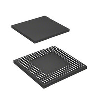
D17760BP200ADV Renesas Electronics America, D17760BP200ADV Datasheet - Page 1173

D17760BP200ADV
Manufacturer Part Number
D17760BP200ADV
Description
MPU 3V 8K,PB-FREE, 256-BGA
Manufacturer
Renesas Electronics America
Series
SuperH® SH7750r
Datasheet
1.D6417760BP200ADV.pdf
(1418 pages)
Specifications of D17760BP200ADV
Core Processor
SH-4
Core Size
32-Bit
Speed
200MHz
Connectivity
Audio Codec, CAN, EBI/EMI, FIFO, I²C, MFI, MMC, SCI, Serial Sound, SIM, SPI, USB
Peripherals
DMA, LCD, POR, WDT
Number Of I /o
69
Program Memory Type
ROMless
Ram Size
48K x 8
Voltage - Supply (vcc/vdd)
1.4 V ~ 1.6 V
Data Converters
A/D 4x10b
Oscillator Type
Internal
Operating Temperature
-40°C ~ 85°C
Package / Case
256-BGA
Lead Free Status / RoHS Status
Lead free / RoHS Compliant
Eeprom Size
-
Program Memory Size
-
Available stocks
Company
Part Number
Manufacturer
Quantity
Price
Company:
Part Number:
D17760BP200ADV
Manufacturer:
Renesas Electronics America
Quantity:
10 000
- Current page: 1173 of 1418
- Download datasheet (9Mb)
30.3.18 LCDC Power-Supply Sequence Period Register (LDPSPR)
LDPSPR controls the power supply circuit that provides power to the LCD module. It sets the
timing for beginning output to the VEPWC and VCPWC pins and for the timing signals which
accompany them.
Initial value:
Bit
15
14
13
12
11
10
9
8
R/W:
Bit:
Bit Name
ONA3
ONA2
ONA1
ONA0
ONB3
ONB2
ONB1
ONB0
ONA3 ONA2 ONA1 ONA0 ONB3 ONB2 ONB1 ONB0 OFFE3 OFFE2 OFFE1 OFFE0 OFFF3 OFFF2 OFFF1 OFFF0
R/W
15
1
R/W
14
1
R/W
13
1
Initial Value
1
1
1
1
0
1
1
0
R/W
12
1
R/W
11
0
R/W
R/W
R/W
R/W
R/W
R/W
R/W
R/W
R/W
R/W
10
1
R/W
9
1
Description
LCDC Power-On Sequence Period
Sets the period from VCPWC assertion to starting
output of the display data (LCD_DATA) and timing
signals (LCD_FLM, LCD_CL1, LCD_CL2, and
LCD_M_DISP) in the power-on sequence of the
LCD module in frame units.
Specify a value of (the period) −1.
This period is the (a) period in figures 30.4 to 30.7,
Power-Supply Control Sequence and States of the
LCD Module.
LCDC Power-On Sequence Period
Sets the period from starting output of the display
data (LCD_DATA) and timing signals (LCD_FLM,
LCD_CL1, LCD_CL2, and LCD_M_DISP) to the
VEPWC assertion in the power-on sequence of the
LCD module in frame units.
Specify a value of (the period) −1.
This period is the (b) period in figures 30.4 to 30.7,
Power-Supply Control Sequence and States of the
LCD Module.
R/W
8
0
R/W
0
7
Rev. 2.00 Feb. 12, 2010 Page 1089 of 1330
R/W
6
0
R/W
5
0
R/W
4
0
R/W
3
1
REJ09B0554-0200
R/W
2
1
R/W
1
1
R/W
0
1
Related parts for D17760BP200ADV
Image
Part Number
Description
Manufacturer
Datasheet
Request
R

Part Number:
Description:
KIT STARTER FOR M16C/29
Manufacturer:
Renesas Electronics America
Datasheet:

Part Number:
Description:
KIT STARTER FOR R8C/2D
Manufacturer:
Renesas Electronics America
Datasheet:

Part Number:
Description:
R0K33062P STARTER KIT
Manufacturer:
Renesas Electronics America
Datasheet:

Part Number:
Description:
KIT STARTER FOR R8C/23 E8A
Manufacturer:
Renesas Electronics America
Datasheet:

Part Number:
Description:
KIT STARTER FOR R8C/25
Manufacturer:
Renesas Electronics America
Datasheet:

Part Number:
Description:
KIT STARTER H8S2456 SHARPE DSPLY
Manufacturer:
Renesas Electronics America
Datasheet:

Part Number:
Description:
KIT STARTER FOR R8C38C
Manufacturer:
Renesas Electronics America
Datasheet:

Part Number:
Description:
KIT STARTER FOR R8C35C
Manufacturer:
Renesas Electronics America
Datasheet:

Part Number:
Description:
KIT STARTER FOR R8CL3AC+LCD APPS
Manufacturer:
Renesas Electronics America
Datasheet:

Part Number:
Description:
KIT STARTER FOR RX610
Manufacturer:
Renesas Electronics America
Datasheet:

Part Number:
Description:
KIT STARTER FOR R32C/118
Manufacturer:
Renesas Electronics America
Datasheet:

Part Number:
Description:
KIT DEV RSK-R8C/26-29
Manufacturer:
Renesas Electronics America
Datasheet:

Part Number:
Description:
KIT STARTER FOR SH7124
Manufacturer:
Renesas Electronics America
Datasheet:

Part Number:
Description:
KIT STARTER FOR H8SX/1622
Manufacturer:
Renesas Electronics America
Datasheet:

Part Number:
Description:
KIT DEV FOR SH7203
Manufacturer:
Renesas Electronics America
Datasheet:


