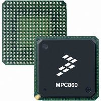
MC68MH360ZP33L Freescale Semiconductor, MC68MH360ZP33L Datasheet - Page 306

MC68MH360ZP33L
Manufacturer Part Number
MC68MH360ZP33L
Description
IC MPU 32BIT QUICC 357-PBGA
Manufacturer
Freescale Semiconductor
Specifications of MC68MH360ZP33L
Processor Type
M683xx 32-Bit
Speed
33MHz
Voltage
5V
Mounting Type
Surface Mount
Package / Case
357-PBGA
Lead Free Status / RoHS Status
Contains lead / RoHS non-compliant
Features
-
Available stocks
Company
Part Number
Manufacturer
Quantity
Price
Company:
Part Number:
MC68MH360ZP33L
Manufacturer:
FREESCALE
Quantity:
1 831
Company:
Part Number:
MC68MH360ZP33L
Manufacturer:
MOTOLOLA
Quantity:
672
Company:
Part Number:
MC68MH360ZP33L
Manufacturer:
Freescale Semiconductor
Quantity:
10 000
Part Number:
MC68MH360ZP33L
Manufacturer:
FREESCALE
Quantity:
20 000
Company:
Part Number:
MC68MH360ZP33LR2
Manufacturer:
Freescale Semiconductor
Quantity:
10 000
- Current page: 306 of 962
- Download datasheet (5Mb)
System Integration Module (SIM60)
6.12.4 DRAM Bank Parity
Parity can be configured for any DRAM bank. Parity is generated and checked on a per-byte
basis using PRTY3–PRTY0 if the PAREN bit is set in the BR. The OPAR bit in the GMR
determines the type of parity (odd or even), and the PBEE bit in the GMR determines if an
internal master should generate an error as a result of a parity error. Any parity error acti-
vates the PERR pin until the associated PERx bit in the MSTAT is cleared.
6.12.5 Refresh Operation
The DRAM controller uses CAS-before-RAS refresh cycles. The refresh cycles are timed
using a dedicated refresh timer. In the CAS-before-RAS method, the DRAMs have an inter-
nal refresh row address counter, so row addresses need not be supplied by the DRAM con-
troller. These DRAMs recognize the assertion of CAS before the assertion of RAS and
perform the refresh using their internal refresh row address value.
Each time the refresh timer expires, the DRAMC performs a refresh cycle. At the first oppor-
tunity after acquiring bus mastership, the DRAM controller requests the bus with the highest
bus arbitration priority level 6. In addition, it asserts the BCLRO signal to minimize the delay
before the refresh cycle begins, assuming the external bus master recognizes this signal
and clears itself off the bus. Once the DRAM controller obtains the bus, it performs a refresh
bus cycle to the DRAM bank.
If more than one bank of DRAM exists in the system, the user should program the refresh
controller to request the bus more often (N times as often, where N is the number of banks).
For instance, typical DRAMs require a refresh every 15.6 s. If 2 banks of DRAM exist in the
system, the DRAM controller should be programmed to refresh every 7.8 s. In the two bank
case, the DRAM controller will alternate between the banks, using the CAS-before-RAS
technique on each bank every 7.8 s.
The DRAM controller will automatically stack up to seven refresh requests before receiving
the bus mastership. Once it receives the bus, it will perform all stacked cycles (up to seven),
as sequential, back-to-back refresh bus cycles.
Refresh cycles are executed only when the RFEN bit in the GMR is set. The refresh cycle
length (three to six clocks) is programmed by the RCYC bits in the GMR. The time between
refreshes is programmed in the RCNT bits in the GMR (see 6.13.1 Global Memory Register
(GMR)).
6-62
Asynchronous external masters do not have parity support.
Parity is not supported for bus cycles terminated with external
assertion of DSACK or TA.
DRAM banks normally need eight read cycles and some delay
time after a power-on reset. After enabling the DRAM bank, the
Freescale Semiconductor, Inc.
For More Information On This Product,
MC68360 USER’S MANUAL
Go to: www.freescale.com
NOTE
NOTE
MOTOROLA
Related parts for MC68MH360ZP33L
Image
Part Number
Description
Manufacturer
Datasheet
Request
R
Part Number:
Description:
Manufacturer:
Freescale Semiconductor, Inc
Datasheet:
Part Number:
Description:
Manufacturer:
Freescale Semiconductor, Inc
Datasheet:
Part Number:
Description:
Manufacturer:
Freescale Semiconductor, Inc
Datasheet:
Part Number:
Description:
Manufacturer:
Freescale Semiconductor, Inc
Datasheet:
Part Number:
Description:
Manufacturer:
Freescale Semiconductor, Inc
Datasheet:
Part Number:
Description:
Manufacturer:
Freescale Semiconductor, Inc
Datasheet:
Part Number:
Description:
Manufacturer:
Freescale Semiconductor, Inc
Datasheet:
Part Number:
Description:
Manufacturer:
Freescale Semiconductor, Inc
Datasheet:
Part Number:
Description:
Manufacturer:
Freescale Semiconductor, Inc
Datasheet:
Part Number:
Description:
Manufacturer:
Freescale Semiconductor, Inc
Datasheet:
Part Number:
Description:
Manufacturer:
Freescale Semiconductor, Inc
Datasheet:
Part Number:
Description:
Manufacturer:
Freescale Semiconductor, Inc
Datasheet:
Part Number:
Description:
Manufacturer:
Freescale Semiconductor, Inc
Datasheet:
Part Number:
Description:
Manufacturer:
Freescale Semiconductor, Inc
Datasheet:
Part Number:
Description:
Manufacturer:
Freescale Semiconductor, Inc
Datasheet:


