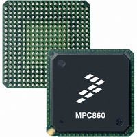
MC68MH360ZP33L Freescale Semiconductor, MC68MH360ZP33L Datasheet - Page 685

MC68MH360ZP33L
Manufacturer Part Number
MC68MH360ZP33L
Description
IC MPU 32BIT QUICC 357-PBGA
Manufacturer
Freescale Semiconductor
Specifications of MC68MH360ZP33L
Processor Type
M683xx 32-Bit
Speed
33MHz
Voltage
5V
Mounting Type
Surface Mount
Package / Case
357-PBGA
Lead Free Status / RoHS Status
Contains lead / RoHS non-compliant
Features
-
Available stocks
Company
Part Number
Manufacturer
Quantity
Price
Company:
Part Number:
MC68MH360ZP33L
Manufacturer:
FREESCALE
Quantity:
1 831
Company:
Part Number:
MC68MH360ZP33L
Manufacturer:
MOTOLOLA
Quantity:
672
Company:
Part Number:
MC68MH360ZP33L
Manufacturer:
Freescale Semiconductor
Quantity:
10 000
Part Number:
MC68MH360ZP33L
Manufacturer:
FREESCALE
Quantity:
20 000
Company:
Part Number:
MC68MH360ZP33LR2
Manufacturer:
Freescale Semiconductor
Quantity:
10 000
- Current page: 685 of 962
- Download datasheet (5Mb)
SCC1
PA4 can be configured as a general-purpose I/O pin, and as an open-drain pin. It may also
be the RXD3 pin for SCC3 in the NMSI mode if the PADIR bit is a zero. It may also be the
L1TXDB pin for TDMb if the PADIR bit is a one. If PA4 is configured as a general-purpose
I/O pin, then the RXD3 input is not defined. If SCC3 is connected to a TDM or is not used,
then PA4 may be used as general-purpose I/O.
PA8 can be configured as a general-purpose I/O pin, but not an open-drain pin. If the corre-
sponding PADIR bit is a zero, it may also be the CLK1 pin (part of the bank of clocks in the
SI), the TIN1 pin (input to timer 1), or the L1RCLKA pin (receive clock to TDMa) or all three
at once. There is no selection between these three inputs in port A, because the connections
are made separately in the SI and the timer mode registers. If the PADIR bit is a one, this
pin may also be the BRGO1 pin (output from BRG1). If the PA8 pin is a general-purpose I/
O pin, then the input to the on-chip peripheral (CLK1, TIN1, or L1RCLKa) is internally con-
nected to BRGO1. See 7.8 Serial Interface with Time Slot Assigner for more details on the
use of the CLK1 and L1RCLKA pins.
PA11 can be configured as a general-purpose I/O pin, but not an open-drain pin. If the
PADIR bit is a zero, PA11 may also be the CLK4 pin (part of the bank of clocks). If the PADIR
bit is a one, PA11 may also be the TOUT2 pin (output from timer 2). If the PA11 pin is a
general-purpose I/O pin, then the input to the on-chip CLK4 function is the value supplied
on the CLK8 pin. This interesting option is useful because not all CLK pins can be routed to
all serial channels in all situations. The ability to send a clock from CLK8 to CLK4 can
increase the flexibility of this assignment process. See 7.8 Serial Interface with Time Slot
Assigner for more details.
MOTOROLA
TO
PADAT
BIT 1
TO
TXD1
OUTPUT
LATCH
MUX
EN
0
1
Figure 7-98. Parallel Block Diagram for PA1
EN
Freescale Semiconductor, Inc.
For More Information On This Product,
16 BITS
PADIR
0
1
MC68360 USER’S MANUAL
Go to: www.freescale.com
MUX
EN
EN
16 BITS
PAPAR
1
0
MUX
EN
16 BITS
PAODR
OPEN
DRAIN
CNTL
EN
Parallel I/O Ports
TXD1/PA1
7-361
PIN
Related parts for MC68MH360ZP33L
Image
Part Number
Description
Manufacturer
Datasheet
Request
R
Part Number:
Description:
Manufacturer:
Freescale Semiconductor, Inc
Datasheet:
Part Number:
Description:
Manufacturer:
Freescale Semiconductor, Inc
Datasheet:
Part Number:
Description:
Manufacturer:
Freescale Semiconductor, Inc
Datasheet:
Part Number:
Description:
Manufacturer:
Freescale Semiconductor, Inc
Datasheet:
Part Number:
Description:
Manufacturer:
Freescale Semiconductor, Inc
Datasheet:
Part Number:
Description:
Manufacturer:
Freescale Semiconductor, Inc
Datasheet:
Part Number:
Description:
Manufacturer:
Freescale Semiconductor, Inc
Datasheet:
Part Number:
Description:
Manufacturer:
Freescale Semiconductor, Inc
Datasheet:
Part Number:
Description:
Manufacturer:
Freescale Semiconductor, Inc
Datasheet:
Part Number:
Description:
Manufacturer:
Freescale Semiconductor, Inc
Datasheet:
Part Number:
Description:
Manufacturer:
Freescale Semiconductor, Inc
Datasheet:
Part Number:
Description:
Manufacturer:
Freescale Semiconductor, Inc
Datasheet:
Part Number:
Description:
Manufacturer:
Freescale Semiconductor, Inc
Datasheet:
Part Number:
Description:
Manufacturer:
Freescale Semiconductor, Inc
Datasheet:
Part Number:
Description:
Manufacturer:
Freescale Semiconductor, Inc
Datasheet:


