TMPSNS-RTD1 Microchip Technology, TMPSNS-RTD1 Datasheet - Page 158
TMPSNS-RTD1
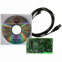
Manufacturer Part Number
TMPSNS-RTD1
Description
BOARD EVAL PT100 RTD TEMP SENSOR
Manufacturer
Microchip Technology
Datasheets
1.MCP3301-CIMS.pdf
(32 pages)
2.PCM18XR1.pdf
(438 pages)
3.MCP6S22DM-PICTL.pdf
(43 pages)
4.TMPSNS-RTD1.pdf
(26 pages)
Specifications of TMPSNS-RTD1
Sensor Type
Temperature
Interface
USB
Embedded
Yes, MCU, 8-Bit
Utilized Ic / Part
MCP3301, MCP6S26, PIC18F2550
Processor To Be Evaluated
MCP6S26, MCP3301, MCP6024, MCP41010, PIC18F2550, TC1071, MCP6002
Data Bus Width
12 bit
Interface Type
USB
Lead Free Status / RoHS Status
Not applicable / Not applicable
Voltage - Supply
-
Sensitivity
-
Sensing Range
-
Lead Free Status / RoHS Status
Lead free / RoHS Compliant, Not applicable / Not applicable


PIC18F2455/2550/4455/4550
16.4.4
In the Half-Bridge Output mode, two pins are used as
outputs to drive push-pull loads. The PWM output sig-
nal is output on the P1A pin, while the complementary
PWM output signal is output on the P1B pin
(Figure 16-4). This mode can be used for half-bridge
applications, as shown in Figure 16-5, or for full-bridge
applications where four power switches are being
modulated with two PWM signals.
In Half-Bridge Output mode, the programmable
dead-band delay can be used to prevent shoot-through
current in half-bridge power devices. The value of bits
PDC6:PDC0 sets the number of instruction cycles
before the output is driven active. If the value is greater
than the duty cycle, the corresponding output remains
inactive during the entire cycle. See Section 16.4.6
“Programmable Dead-Band Delay” for more details
of the dead-band delay operations.
Since the P1A and P1B outputs are multiplexed with
the PORTC<2> and PORTD<5> data latches, the
TRISC<2> and TRISD<5> bits must be cleared to
configure P1A and P1B as outputs.
FIGURE 16-5:
DS39632E-page 156
Standard Half-Bridge Circuit (“Push-Pull”)
Half-Bridge Output Driving a Full-Bridge Circuit
HALF-BRIDGE MODE
EXAMPLES OF HALF-BRIDGE OUTPUT MODE APPLICATIONS
PIC18FX455/X550
P1A
P1B
PIC18FX455/X550
P1A
P1B
FET
Driver
FET
Driver
FET
Driver
FET
Driver
FIGURE 16-4:
Note 1: At this time, the TMR2 register is equal to the
P1A
P1B
td = Dead-Band Delay
(2)
(2)
2: Output signals are shown as active-high.
(1)
Load
V+
PR2 register.
V-
td
V+
V-
Duty Cycle
Period
Load
td
HALF-BRIDGE PWM
OUTPUT
© 2009 Microchip Technology Inc.
FET
Driver
FET
Driver
(1)
+
V
-
+
V
-
Period
(1)
Related parts for TMPSNS-RTD1
Image
Part Number
Description
Manufacturer
Datasheet
Request
R

Part Number:
Description:
Manufacturer:
Microchip Technology Inc.
Datasheet:
Part Number:
Description:
Manufacturer:
Microchip Technology Inc.
Datasheet:
Part Number:
Description:
Manufacturer:
Microchip Technology Inc.
Datasheet:
Part Number:
Description:
Manufacturer:
Microchip Technology Inc.
Datasheet:
Part Number:
Description:
Manufacturer:
Microchip Technology Inc.
Datasheet:
Part Number:
Description:
Manufacturer:
Microchip Technology Inc.
Datasheet:
Part Number:
Description:
Manufacturer:
Microchip Technology Inc.
Datasheet:
Part Number:
Description:
Manufacturer:
Microchip Technology Inc.
Datasheet: