TMPSNS-RTD1 Microchip Technology, TMPSNS-RTD1 Datasheet - Page 349
TMPSNS-RTD1
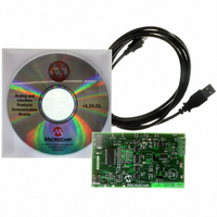
Manufacturer Part Number
TMPSNS-RTD1
Description
BOARD EVAL PT100 RTD TEMP SENSOR
Manufacturer
Microchip Technology
Datasheets
1.MCP3301-CIMS.pdf
(32 pages)
2.PCM18XR1.pdf
(438 pages)
3.MCP6S22DM-PICTL.pdf
(43 pages)
4.TMPSNS-RTD1.pdf
(26 pages)
Specifications of TMPSNS-RTD1
Sensor Type
Temperature
Interface
USB
Embedded
Yes, MCU, 8-Bit
Utilized Ic / Part
MCP3301, MCP6S26, PIC18F2550
Processor To Be Evaluated
MCP6S26, MCP3301, MCP6024, MCP41010, PIC18F2550, TC1071, MCP6002
Data Bus Width
12 bit
Interface Type
USB
Lead Free Status / RoHS Status
Not applicable / Not applicable
Voltage - Supply
-
Sensitivity
-
Sensing Range
-
Lead Free Status / RoHS Status
Lead free / RoHS Compliant, Not applicable / Not applicable


RRNCF
Syntax:
Operands:
Operation:
Status Affected:
Encoding:
Description:
Words:
Cycles:
Example 1:
Example 2:
© 2009 Microchip Technology Inc.
Q Cycle Activity:
Before Instruction
After Instruction
Before Instruction
After Instruction
Decode
REG
REG
W
REG
W
REG
Q1
=
=
=
=
=
=
register ‘f’
Rotate Right f (No Carry)
RRNCF
0 ≤ f ≤ 255
d ∈ [0,1]
a ∈ [0,1]
(f<n>) → dest<n – 1>,
(f<0>) → dest<7>
N, Z
The contents of register ‘f’ are rotated
one bit to the right. If ‘d’ is ‘0’, the result
is placed in W. If ‘d’ is ‘1’, the result is
placed back in register ‘f’ (default).
If ‘a’ is ‘0’, the Access Bank will be
selected, overriding the BSR value. If ‘a’
is ‘1’, then the bank will be selected as
per the BSR value (default).
If ‘a’ is ‘0’ and the extended instruction
set is enabled, this instruction operates
in Indexed Literal Offset Addressing
mode whenever f ≤ 95 (5Fh). See
Section 26.2.3 “Byte-Oriented and
Bit-Oriented Instructions in Indexed
Literal Offset Mode” for details.
1
1
RRNCF
RRNCF
Read
0100
Q2
1101 0111
1110 1011
?
1101 0111
1110 1011
1101 0111
f {,d {,a}}
REG, 1, 0
REG, 0, 0
00da
Process
Data
Q3
register f
ffff
destination
Write to
PIC18F2455/2550/4455/4550
Q4
ffff
SETF
Syntax:
Operands:
Operation:
Status Affected:
Encoding:
Description:
Words:
Cycles:
Example:
Q Cycle Activity:
Before Instruction
After Instruction
Decode
REG
REG
Q1
register ‘f’
Set f
SETF
0 ≤ f ≤ 255
a ∈ [0,1]
FFh → f
None
The contents of the specified register
are set to FFh.
If ‘a’ is ‘0’, the Access Bank is selected.
If ‘a’ is ‘1’, the BSR is used to select the
GPR bank (default).
If ‘a’ is ‘0’ and the extended instruction
set is enabled, this instruction operates
in Indexed Literal Offset Addressing
mode whenever f ≤ 95 (5Fh). See
Section 26.2.3 “Byte-Oriented and
Bit-Oriented Instructions in Indexed
Literal Offset Mode” for details.
1
1
SETF
Read
0110
Q2
=
=
f {,a}
5Ah
FFh
100a
Process
Data
REG,1
Q3
DS39632E-page 347
ffff
register ‘f’
Write
Q4
ffff
Related parts for TMPSNS-RTD1
Image
Part Number
Description
Manufacturer
Datasheet
Request
R

Part Number:
Description:
Manufacturer:
Microchip Technology Inc.
Datasheet:
Part Number:
Description:
Manufacturer:
Microchip Technology Inc.
Datasheet:
Part Number:
Description:
Manufacturer:
Microchip Technology Inc.
Datasheet:
Part Number:
Description:
Manufacturer:
Microchip Technology Inc.
Datasheet:
Part Number:
Description:
Manufacturer:
Microchip Technology Inc.
Datasheet:
Part Number:
Description:
Manufacturer:
Microchip Technology Inc.
Datasheet:
Part Number:
Description:
Manufacturer:
Microchip Technology Inc.
Datasheet:
Part Number:
Description:
Manufacturer:
Microchip Technology Inc.
Datasheet: