TMPSNS-RTD1 Microchip Technology, TMPSNS-RTD1 Datasheet - Page 23
TMPSNS-RTD1
Manufacturer Part Number
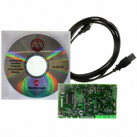
TMPSNS-RTD1
Description
BOARD EVAL PT100 RTD TEMP SENSOR
Manufacturer
Microchip Technology
Datasheets
1.MCP3301-CIMS.pdf
(32 pages)
2.PCM18XR1.pdf
(438 pages)
3.MCP6S22DM-PICTL.pdf
(43 pages)
4.TMPSNS-RTD1.pdf
(26 pages)
Specifications of TMPSNS-RTD1
Sensor Type
Temperature
Interface
USB
Embedded
Yes, MCU, 8-Bit
Utilized Ic / Part
MCP3301, MCP6S26, PIC18F2550
Processor To Be Evaluated
MCP6S26, MCP3301, MCP6024, MCP41010, PIC18F2550, TC1071, MCP6002
Data Bus Width
12 bit
Interface Type
USB
Lead Free Status / RoHS Status
Not applicable / Not applicable
Voltage - Supply
-
Sensitivity
-
Sensing Range
-
Lead Free Status / RoHS Status
Lead free / RoHS Compliant, Not applicable / Not applicable


TABLE 1-3:
© 2009 Microchip Technology Inc.
RE0/AN5/CK1SPP
RE1/AN6/CK2SPP
RE2/AN7/OESPP
RE3
V
V
V
NC/ICCK/ICPGC
NC/ICDT/ICPGD
NC/ICRST/ICV
NC/ICPORTS
NC
Legend: TTL = TTL compatible input
Note 1:
USB
SS
DD
RE0
AN5
CK1SPP
RE1
AN6
CK2SPP
RE2
AN7
OESPP
ICCK
ICPGC
ICDT
ICPGD
ICRST
ICV
ICPORTS
2:
3:
Pin Name
PP
ST = Schmitt Trigger input with CMOS levels
O
Alternate assignment for CCP2 when CCP2MX Configuration bit is cleared.
Default assignment for CCP2 when CCP2MX Configuration bit is set.
These pins are No Connect unless the ICPRT Configuration bit is set. For NC/ICPORTS, the pin is No
Connect unless ICPRT is set and the DEBUG Configuration bit is cleared.
(3)
PP
= Output
(3)
(3)
(3)
PIC18F4455/4550 PINOUT I/O DESCRIPTIONS (CONTINUED)
12, 31 6, 30,
11, 32 7, 8,
PDIP QFN TQFP
10
18
—
—
—
—
—
—
8
9
Pin Number
28, 29
25
26
27
31
37
13
—
—
—
—
—
6, 29
7, 28
25
26
27
37
12
13
33
34
—
—
PIC18F2455/2550/4455/4550
Type
Pin
I/O
I/O
I/O
I/O
I/O
I/O
I/O
—
—
O
O
O
P
P
P
P
P
I
I
I
I
Analog
Analog
Analog
Buffer
Type
ST
ST
ST
ST
ST
ST
ST
—
—
—
—
—
—
—
—
—
—
—
CMOS = CMOS compatible input or output
I
P
PORTE is a bidirectional I/O port.
See MCLR/V
Ground reference for logic and I/O pins.
Positive supply for logic and I/O pins.
Internal USB 3.3V voltage regulator output, positive
supply for the USB transceiver.
No Connect or dedicated ICD/ICSP™ port clock.
No Connect or dedicated ICD/ICSP port clock.
No Connect or dedicated ICD/ICSP port Reset.
No Connect or 28-pin device emulation.
No Connect.
Digital I/O.
Analog input 5.
SPP clock 1 output.
Digital I/O.
Analog input 6.
SPP clock 2 output.
Digital I/O.
Analog input 7.
SPP output enable output.
In-Circuit Debugger clock.
ICSP programming clock.
In-Circuit Debugger data.
ICSP programming data.
Master Clear (Reset) input.
Programming voltage input.
Enable 28-pin device emulation when connected
to V
= Input
= Power
SS
.
PP
/RE3 pin.
Description
DS39632E-page 21
Related parts for TMPSNS-RTD1
Image
Part Number
Description
Manufacturer
Datasheet
Request
R

Part Number:
Description:
Manufacturer:
Microchip Technology Inc.
Datasheet:
Part Number:
Description:
Manufacturer:
Microchip Technology Inc.
Datasheet:
Part Number:
Description:
Manufacturer:
Microchip Technology Inc.
Datasheet:
Part Number:
Description:
Manufacturer:
Microchip Technology Inc.
Datasheet:
Part Number:
Description:
Manufacturer:
Microchip Technology Inc.
Datasheet:
Part Number:
Description:
Manufacturer:
Microchip Technology Inc.
Datasheet:
Part Number:
Description:
Manufacturer:
Microchip Technology Inc.
Datasheet:
Part Number:
Description:
Manufacturer:
Microchip Technology Inc.
Datasheet: