TMPSNS-RTD1 Microchip Technology, TMPSNS-RTD1 Datasheet - Page 270
TMPSNS-RTD1
Manufacturer Part Number
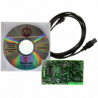
TMPSNS-RTD1
Description
BOARD EVAL PT100 RTD TEMP SENSOR
Manufacturer
Microchip Technology
Datasheets
1.MCP3301-CIMS.pdf
(32 pages)
2.PCM18XR1.pdf
(438 pages)
3.MCP6S22DM-PICTL.pdf
(43 pages)
4.TMPSNS-RTD1.pdf
(26 pages)
Specifications of TMPSNS-RTD1
Sensor Type
Temperature
Interface
USB
Embedded
Yes, MCU, 8-Bit
Utilized Ic / Part
MCP3301, MCP6S26, PIC18F2550
Processor To Be Evaluated
MCP6S26, MCP3301, MCP6024, MCP41010, PIC18F2550, TC1071, MCP6002
Data Bus Width
12 bit
Interface Type
USB
Lead Free Status / RoHS Status
Not applicable / Not applicable
Voltage - Supply
-
Sensitivity
-
Sensing Range
-
Lead Free Status / RoHS Status
Lead free / RoHS Compliant, Not applicable / Not applicable


PIC18F2455/2550/4455/4550
The analog reference voltage is software selectable to
either the device’s positive and negative supply voltage
(V
RA3/AN3/V
The A/D converter has a unique feature of being able
to operate while the device is in Sleep mode. To
operate in Sleep, the A/D conversion clock must be
derived from the A/D’s internal RC oscillator.
The output of the sample and hold is the input into the
converter, which generates the result via successive
approximation.
FIGURE 21-1:
DS39632E-page 268
DD
Note 1:
and V
REF
2:
SS
+ and RA2/AN2/V
Converter
) or the voltage level on the
10-Bit
Channels AN5 through AN7 are not available on 28-pin devices.
I/O pins have diode protection to V
A/D
Reference
Voltage
A/D BLOCK DIAGRAM
REF
-/CV
V
V
REF
REF
REF
+
-
(Input Voltage)
pins.
VCFG1:VCFG0
V
AIN
DD
and V
X
X
1
0
0
1
X
X
V
SS
DD
A device Reset forces all registers to their Reset state.
This forces the A/D module to be turned off and any
conversion in progress is aborted.
Each port pin associated with the A/D converter can be
configured as an analog input or as a digital I/O. The
ADRESH and ADRESL registers contain the result of
the A/D conversion. When the A/D conversion is com-
plete, the result is loaded into the ADRESH:ADRESL
register pair, the GO/DONE bit (ADCON0 register) is
cleared and A/D Interrupt Flag bit, ADIF, is set. The
block diagram of the A/D module is shown in
Figure 21-1.
.
(2)
V
SS (2)
CHS3:CHS0
1100
1011
1010
1001
1000
0111
0110
0101
0100
0011
0010
0001
0000
© 2009 Microchip Technology Inc.
AN12
AN11
AN10
AN9
AN8
AN7
AN6
AN5
AN4
AN3
AN2
AN1
AN0
(1)
(1)
(1)
Related parts for TMPSNS-RTD1
Image
Part Number
Description
Manufacturer
Datasheet
Request
R

Part Number:
Description:
Manufacturer:
Microchip Technology Inc.
Datasheet:
Part Number:
Description:
Manufacturer:
Microchip Technology Inc.
Datasheet:
Part Number:
Description:
Manufacturer:
Microchip Technology Inc.
Datasheet:
Part Number:
Description:
Manufacturer:
Microchip Technology Inc.
Datasheet:
Part Number:
Description:
Manufacturer:
Microchip Technology Inc.
Datasheet:
Part Number:
Description:
Manufacturer:
Microchip Technology Inc.
Datasheet:
Part Number:
Description:
Manufacturer:
Microchip Technology Inc.
Datasheet:
Part Number:
Description:
Manufacturer:
Microchip Technology Inc.
Datasheet: