TMPSNS-RTD1 Microchip Technology, TMPSNS-RTD1 Datasheet - Page 425
TMPSNS-RTD1
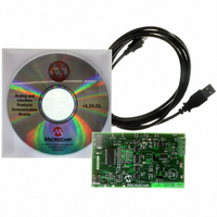
Manufacturer Part Number
TMPSNS-RTD1
Description
BOARD EVAL PT100 RTD TEMP SENSOR
Manufacturer
Microchip Technology
Datasheets
1.MCP3301-CIMS.pdf
(32 pages)
2.PCM18XR1.pdf
(438 pages)
3.MCP6S22DM-PICTL.pdf
(43 pages)
4.TMPSNS-RTD1.pdf
(26 pages)
Specifications of TMPSNS-RTD1
Sensor Type
Temperature
Interface
USB
Embedded
Yes, MCU, 8-Bit
Utilized Ic / Part
MCP3301, MCP6S26, PIC18F2550
Processor To Be Evaluated
MCP6S26, MCP3301, MCP6024, MCP41010, PIC18F2550, TC1071, MCP6002
Data Bus Width
12 bit
Interface Type
USB
Lead Free Status / RoHS Status
Not applicable / Not applicable
Voltage - Supply
-
Sensitivity
-
Sensing Range
-
Lead Free Status / RoHS Status
Lead free / RoHS Compliant, Not applicable / Not applicable


INDEX
A
A/D ................................................................................... 265
Absolute Maximum Ratings ............................................. 367
AC (Timing) Characteristics ............................................. 385
AC Characteristics
Access Bank
ACKSTAT ........................................................................ 232
ACKSTAT Status Flag ..................................................... 232
ADCON0 Register ............................................................ 265
ADCON1 Register ............................................................ 265
ADCON2 Register ............................................................ 265
ADDFSR .......................................................................... 356
ADDLW ............................................................................ 319
ADDULNK ........................................................................ 356
ADDWF ............................................................................ 319
ADDWFC ......................................................................... 320
ADRESH Register ............................................................ 265
ADRESL Register .................................................... 265, 268
Analog-to-Digital Converter. See A/D.
and BSR ............................................................................. 79
ANDLW ............................................................................ 320
ANDWF ............................................................................ 321
Assembler
B
Baud Rate Generator ....................................................... 228
BC .................................................................................... 321
BCF .................................................................................. 322
BF .................................................................................... 232
BF Status Flag ................................................................. 232
© 2009 Microchip Technology Inc.
Acquisition Requirements ........................................ 270
ADCON0 Register .................................................... 265
ADCON1 Register .................................................... 265
ADCON2 Register .................................................... 265
ADRESH Register ............................................ 265, 268
ADRESL Register .................................................... 265
Analog Port Pins, Configuring .................................. 272
Associated Registers ............................................... 274
Configuring the Module ............................................ 269
Conversion Clock (T
Conversion Requirements ....................................... 405
Conversion Status (GO/DONE Bit) .......................... 268
Conversions ............................................................. 273
Converter Characteristics ........................................ 404
Converter Interrupt, Configuring .............................. 269
Discharge ................................................................. 273
Operation in Power-Managed Modes ...................... 272
Selecting and Configuring Acquisition Time ............ 271
Special Event Trigger (CCP2) .................................. 274
Special Event Trigger (ECCP) ................................. 152
Use of the CCP2 Trigger .......................................... 274
Load Conditions for Device Timing
Parameter Symbology ............................................. 385
Temperature and Voltage Specifications ................. 386
Timing Conditions .................................................... 386
Internal RC Accuracy ............................................... 388
Mapping with Indexed Literal Offset Mode ................. 79
GO/DONE Bit ........................................................... 268
MPASM Assembler .................................................. 364
Specifications ................................................... 386
AD
) ........................................... 271
PIC18F2455/2550/4455/4550
Block Diagrams
BN .................................................................................... 322
BNC ................................................................................. 323
BNN ................................................................................. 323
BNOV .............................................................................. 324
BNZ ................................................................................. 324
BOR. See Brown-out Reset.
BOV ................................................................................. 327
BRA ................................................................................. 325
Break Character (12-Bit) Transmit and Receive .............. 259
BRG. See Baud Rate Generator.
Brown-out Reset (BOR) ..................................................... 48
BSF .................................................................................. 325
BTFSC ............................................................................. 326
BTFSS ............................................................................. 326
BTG ................................................................................. 327
BZ .................................................................................... 328
A/D ........................................................................... 268
Analog Input Model .................................................. 269
Baud Rate Generator .............................................. 228
Capture Mode Operation ......................................... 145
Comparator Analog Input Model .............................. 279
Comparator I/O Operating Modes ........................... 276
Comparator Output .................................................. 278
Comparator Voltage Reference ............................... 282
Comparator Voltage Reference
Compare Mode Operation ....................................... 146
Device Clock .............................................................. 24
Enhanced PWM ....................................................... 153
EUSART Receive .................................................... 257
EUSART Transmit ................................................... 254
External Power-on Reset Circuit
Fail-Safe Clock Monitor ........................................... 306
Generic I/O Port ....................................................... 113
High/Low-Voltage Detect with External Input .......... 286
Interrupt Logic .......................................................... 100
MSSP (I
MSSP (I
MSSP (SPI Mode) ................................................... 197
On-Chip Reset Circuit ................................................ 45
PIC18F2455/2550 ..................................................... 10
PIC18F4455/4550 ..................................................... 11
PLL (HS Mode) .......................................................... 27
PWM Operation (Simplified) .................................... 148
Reads from Flash Program Memory ......................... 85
Single Comparator ................................................... 277
SPP Data Path ........................................................ 191
Table Read Operation ............................................... 81
Table Write Operation ............................................... 82
Table Writes to Flash Program Memory .................... 87
Timer0 in 16-Bit Mode ............................................. 128
Timer0 in 8-Bit Mode ............................................... 128
Timer1 ..................................................................... 132
Timer1 (16-Bit Read/Write Mode) ............................ 132
Timer2 ..................................................................... 138
Timer3 ..................................................................... 140
Timer3 (16-Bit Read/Write Mode) ............................ 140
USB Interrupt Logic ................................................. 180
USB Peripheral and Options ................................... 165
Watchdog Timer ...................................................... 303
Detecting ................................................................... 48
Disabling in Sleep Mode ............................................ 48
Software Enabled ...................................................... 48
Output Buffer Example .................................... 283
(Slow V
2
2
C Master Mode) ........................................ 226
C Mode) .................................................... 207
DD
Power-up) ........................................ 47
DS39632E-page 423
Related parts for TMPSNS-RTD1
Image
Part Number
Description
Manufacturer
Datasheet
Request
R

Part Number:
Description:
Manufacturer:
Microchip Technology Inc.
Datasheet:
Part Number:
Description:
Manufacturer:
Microchip Technology Inc.
Datasheet:
Part Number:
Description:
Manufacturer:
Microchip Technology Inc.
Datasheet:
Part Number:
Description:
Manufacturer:
Microchip Technology Inc.
Datasheet:
Part Number:
Description:
Manufacturer:
Microchip Technology Inc.
Datasheet:
Part Number:
Description:
Manufacturer:
Microchip Technology Inc.
Datasheet:
Part Number:
Description:
Manufacturer:
Microchip Technology Inc.
Datasheet:
Part Number:
Description:
Manufacturer:
Microchip Technology Inc.
Datasheet: