TMPSNS-RTD1 Microchip Technology, TMPSNS-RTD1 Datasheet - Page 206
TMPSNS-RTD1
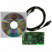
Manufacturer Part Number
TMPSNS-RTD1
Description
BOARD EVAL PT100 RTD TEMP SENSOR
Manufacturer
Microchip Technology
Datasheets
1.MCP3301-CIMS.pdf
(32 pages)
2.PCM18XR1.pdf
(438 pages)
3.MCP6S22DM-PICTL.pdf
(43 pages)
4.TMPSNS-RTD1.pdf
(26 pages)
Specifications of TMPSNS-RTD1
Sensor Type
Temperature
Interface
USB
Embedded
Yes, MCU, 8-Bit
Utilized Ic / Part
MCP3301, MCP6S26, PIC18F2550
Processor To Be Evaluated
MCP6S26, MCP3301, MCP6024, MCP41010, PIC18F2550, TC1071, MCP6002
Data Bus Width
12 bit
Interface Type
USB
Lead Free Status / RoHS Status
Not applicable / Not applicable
Voltage - Supply
-
Sensitivity
-
Sensing Range
-
Lead Free Status / RoHS Status
Lead free / RoHS Compliant, Not applicable / Not applicable


PIC18F2455/2550/4455/4550
19.3.6
In Slave mode, the data is transmitted and received as
the external clock pulses appear on SCK. When the
last bit is latched, the SSPIF interrupt flag bit is set.
While in Slave mode, the external clock is supplied by
the external clock source on the SCK pin. This external
clock must meet the minimum high and low times as
specified in the electrical specifications.
While in Sleep mode, the slave can transmit/receive
data. When a byte is received, the device can be con-
figured to wake-up from Sleep.
19.3.7
The SS pin allows a Synchronous Slave mode. The
SPI must be in Slave mode with the SS pin control
enabled (SSPCON1<3:0> = 04h). When the SS pin is
low, transmission and reception are enabled and the
SDO pin is driven. When the SS pin goes high, the
SDO pin is no longer driven, even if in the middle of a
FIGURE 19-4:
DS39632E-page 204
SCK
(CKP = 0
CKE = 0)
SCK
(CKP = 1
CKE = 0)
Write to
SSPBUF
SDO
SDI
(SMP = 0)
Input
Sample
(SMP = 0)
SSPIF
Interrupt
Flag
SSPSR to
SSPBUF
SS
SLAVE MODE
SLAVE SELECT
SYNCHRONIZATION
SLAVE SYNCHRONIZATION WAVEFORM
bit 7
bit 7
bit 6
transmitted byte and becomes a floating output. Exter-
nal pull-up/pull-down resistors may be desirable
depending on the application.
When the SPI module resets, the bit counter is forced
to ‘0’. This can be done by either forcing the SS pin to
a high level or clearing the SSPEN bit.
To emulate two-wire communication, the SDO pin can
be connected to the SDI pin. When the SPI needs to
operate as a receiver, the SDO pin can be configured
as an input. This disables transmissions from the SDO.
The SDI can always be left as an input (SDI function)
since it cannot create a bus conflict.
Note 1: When the SPI module is in Slave mode
2: If the SPI is used in Slave mode with CKE
with
(SSPCON1<3:0> = 0100), the SPI module
will reset if the SS pin is set to V
set, then the SS pin control must be
enabled.
bit 7
bit 7
SS
© 2009 Microchip Technology Inc.
pin
Next Q4 Cycle
after Q2↓
control
bit 0
bit 0
DD
enabled
.
Related parts for TMPSNS-RTD1
Image
Part Number
Description
Manufacturer
Datasheet
Request
R

Part Number:
Description:
Manufacturer:
Microchip Technology Inc.
Datasheet:
Part Number:
Description:
Manufacturer:
Microchip Technology Inc.
Datasheet:
Part Number:
Description:
Manufacturer:
Microchip Technology Inc.
Datasheet:
Part Number:
Description:
Manufacturer:
Microchip Technology Inc.
Datasheet:
Part Number:
Description:
Manufacturer:
Microchip Technology Inc.
Datasheet:
Part Number:
Description:
Manufacturer:
Microchip Technology Inc.
Datasheet:
Part Number:
Description:
Manufacturer:
Microchip Technology Inc.
Datasheet:
Part Number:
Description:
Manufacturer:
Microchip Technology Inc.
Datasheet: