TMPSNS-RTD1 Microchip Technology, TMPSNS-RTD1 Datasheet - Page 428
TMPSNS-RTD1
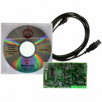
Manufacturer Part Number
TMPSNS-RTD1
Description
BOARD EVAL PT100 RTD TEMP SENSOR
Manufacturer
Microchip Technology
Datasheets
1.MCP3301-CIMS.pdf
(32 pages)
2.PCM18XR1.pdf
(438 pages)
3.MCP6S22DM-PICTL.pdf
(43 pages)
4.TMPSNS-RTD1.pdf
(26 pages)
Specifications of TMPSNS-RTD1
Sensor Type
Temperature
Interface
USB
Embedded
Yes, MCU, 8-Bit
Utilized Ic / Part
MCP3301, MCP6S26, PIC18F2550
Processor To Be Evaluated
MCP6S26, MCP3301, MCP6024, MCP41010, PIC18F2550, TC1071, MCP6002
Data Bus Width
12 bit
Interface Type
USB
Lead Free Status / RoHS Status
Not applicable / Not applicable
Voltage - Supply
-
Sensitivity
-
Sensing Range
-
Lead Free Status / RoHS Status
Lead free / RoHS Compliant, Not applicable / Not applicable


PIC18F2455/2550/4455/4550
High/Low-Voltage Detect ................................................. 285
HLVD. See High/Low-Voltage Detect. ............................. 285
I
I/O Ports ........................................................................... 113
I
ID Locations ............................................................. 291, 311
Idle Modes .......................................................................... 40
INCF ................................................................................. 334
INCFSZ ............................................................................ 335
In-Circuit Debugger .......................................................... 311
In-Circuit Serial Programming (ICSP) ...................... 291, 311
Indexed Literal Offset Addressing
Indexed Literal Offset Mode ................................. 77, 79, 360
Indirect Addressing ............................................................ 75
INFSNZ ............................................................................ 335
Initialization Conditions for all Registers ...................... 53–57
DS39632E-page 426
2
C Mode (MSSP)
Applications .............................................................. 288
Associated Registers ............................................... 289
Characteristics ......................................................... 384
Current Consumption ............................................... 287
Effects of a Reset ..................................................... 289
Operation ................................................................. 286
Setup ........................................................................ 287
Start-up Time ........................................................... 287
Typical Application ................................................... 288
Acknowledge Sequence Timing ............................... 235
Associated Registers ............................................... 241
Baud Rate Generator ............................................... 228
Bus Collision
Clock Arbitration ....................................................... 229
Clock Stretching ....................................................... 221
Clock Synchronization and the CKP Bit ................... 222
Effect of a Reset ...................................................... 236
General Call Address Support ................................. 225
I
Master Mode ............................................................ 226
Multi-Master Communication, Bus Collision
Multi-Master Mode ................................................... 236
Operation ................................................................. 212
Read/Write Bit Information (R/W Bit) ............... 212, 214
Registers .................................................................. 207
Serial Clock (RB1/AN10/INT1/SCK/SCL) ................ 214
Slave Mode .............................................................. 212
Sleep Operation ....................................................... 236
Stop Condition Timing .............................................. 235
and Standard PIC18 Instructions ............................. 360
2
C Clock Rate w/BRG ............................................. 228
During Sleep .................................................... 289
During a Repeated Start Condition .................. 239
During a Stop Condition ................................... 240
10-Bit Slave Receive Mode (SEN = 1) ............. 221
10-Bit Slave Transmit Mode ............................. 221
7-Bit Slave Receive Mode (SEN = 1) ............... 221
7-Bit Slave Transmit Mode ............................... 221
Operation ......................................................... 227
Reception ......................................................... 232
Repeated Start Condition Timing ..................... 231
Start Condition Timing ..................................... 230
Transmission .................................................... 232
Transmit Sequence .......................................... 227
and Arbitration .................................................. 236
Addressing ....................................................... 212
Addressing Masking ......................................... 213
Reception ......................................................... 214
Transmission .................................................... 214
Instruction Cycle ................................................................ 63
Instruction Set .................................................................. 313
Clocking Scheme ....................................................... 63
Flow/Pipelining ........................................................... 63
ADDLW .................................................................... 319
ADDWF .................................................................... 319
ADDWF (Indexed Literal Offset mode) .................... 361
ADDWFC ................................................................. 320
ANDLW .................................................................... 320
ANDWF .................................................................... 321
BC ............................................................................ 321
BCF ......................................................................... 322
BN ............................................................................ 322
BNC ......................................................................... 323
BNN ......................................................................... 323
BNOV ...................................................................... 324
BNZ ......................................................................... 324
BOV ......................................................................... 327
BRA ......................................................................... 325
BSF .......................................................................... 325
BSF (Indexed Literal Offset mode) .......................... 361
BTFSC ..................................................................... 326
BTFSS ..................................................................... 326
BTG ......................................................................... 327
BZ ............................................................................ 328
CALL ........................................................................ 328
CLRF ....................................................................... 329
CLRWDT ................................................................. 329
COMF ...................................................................... 330
CPFSEQ .................................................................. 330
CPFSGT .................................................................. 331
CPFSLT ................................................................... 331
DAW ........................................................................ 332
DCFSNZ .................................................................. 333
DECF ....................................................................... 332
DECFSZ .................................................................. 333
General Format ........................................................ 315
GOTO ...................................................................... 334
INCF ........................................................................ 334
INCFSZ .................................................................... 335
INFSNZ .................................................................... 335
IORLW ..................................................................... 336
IORWF ..................................................................... 336
LFSR ....................................................................... 337
MOVF ...................................................................... 337
MOVFF .................................................................... 338
MOVLB .................................................................... 338
MOVLW ................................................................... 339
MOVWF ................................................................... 339
MULLW .................................................................... 340
MULWF .................................................................... 340
NEGF ....................................................................... 341
NOP ......................................................................... 341
Opcode Field Descriptions ....................................... 314
POP ......................................................................... 342
PUSH ....................................................................... 342
RCALL ..................................................................... 343
RESET ..................................................................... 343
RETFIE .................................................................... 344
RETLW .................................................................... 344
RETURN .................................................................. 345
RLCF ....................................................................... 345
RLNCF ..................................................................... 346
RRCF ....................................................................... 346
RRNCF .................................................................... 347
© 2009 Microchip Technology Inc.
Related parts for TMPSNS-RTD1
Image
Part Number
Description
Manufacturer
Datasheet
Request
R

Part Number:
Description:
Manufacturer:
Microchip Technology Inc.
Datasheet:
Part Number:
Description:
Manufacturer:
Microchip Technology Inc.
Datasheet:
Part Number:
Description:
Manufacturer:
Microchip Technology Inc.
Datasheet:
Part Number:
Description:
Manufacturer:
Microchip Technology Inc.
Datasheet:
Part Number:
Description:
Manufacturer:
Microchip Technology Inc.
Datasheet:
Part Number:
Description:
Manufacturer:
Microchip Technology Inc.
Datasheet:
Part Number:
Description:
Manufacturer:
Microchip Technology Inc.
Datasheet:
Part Number:
Description:
Manufacturer:
Microchip Technology Inc.
Datasheet: