TMPSNS-RTD1 Microchip Technology, TMPSNS-RTD1 Datasheet - Page 199
TMPSNS-RTD1
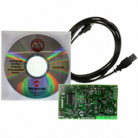
Manufacturer Part Number
TMPSNS-RTD1
Description
BOARD EVAL PT100 RTD TEMP SENSOR
Manufacturer
Microchip Technology
Datasheets
1.MCP3301-CIMS.pdf
(32 pages)
2.PCM18XR1.pdf
(438 pages)
3.MCP6S22DM-PICTL.pdf
(43 pages)
4.TMPSNS-RTD1.pdf
(26 pages)
Specifications of TMPSNS-RTD1
Sensor Type
Temperature
Interface
USB
Embedded
Yes, MCU, 8-Bit
Utilized Ic / Part
MCP3301, MCP6S26, PIC18F2550
Processor To Be Evaluated
MCP6S26, MCP3301, MCP6024, MCP41010, PIC18F2550, TC1071, MCP6002
Data Bus Width
12 bit
Interface Type
USB
Lead Free Status / RoHS Status
Not applicable / Not applicable
Voltage - Supply
-
Sensitivity
-
Sensing Range
-
Lead Free Status / RoHS Status
Lead free / RoHS Compliant, Not applicable / Not applicable


19.0
19.1
The Master Synchronous Serial Port (MSSP) module is
a serial interface, useful for communicating with other
peripheral or microcontroller devices. These peripheral
devices may be serial EEPROMs, shift registers,
display drivers, A/D converters, etc. The MSSP module
can operate in one of two modes:
• Serial Peripheral Interface (SPI)
• Inter-Integrated Circuit (I
The I
hardware:
• Master mode
• Multi-Master mode
• Slave mode
19.2
The MSSP module has three associated control regis-
ters. These include a status register (SSPSTAT) and
two control registers (SSPCON1 and SSPCON2). The
use of these registers and their individual Configuration
bits differ significantly depending on whether the MSSP
module is operated in SPI or I
Additional details are provided under the individual
sections.
© 2009 Microchip Technology Inc.
- Full Master mode
- Slave mode (with general address call)
2
C interface supports the following modes in
MASTER SYNCHRONOUS
SERIAL PORT (MSSP)
MODULE
Master SSP (MSSP) Module
Overview
Control Registers
2
C™)
2
C mode.
PIC18F2455/2550/4455/4550
19.3
The SPI mode allows 8 bits of data to be synchronously
transmitted and received simultaneously. All four
modes of the SPI are supported. To accomplish
communication, typically three pins are used:
• Serial Data Out (SDO) – RC7/RX/DT/SDO
• Serial Data In (SDI) – RB0/AN12/INT0/FLT0/SDI/SDA
• Serial Clock (SCK) – RB1/AN10/INT1/SCK/SCL
Additionally, a fourth pin may be used when in a Slave
mode of operation:
• Slave Select (SS) – RA5/AN4/SS/HLVDIN/C2OUT
Figure 19-1 shows the block diagram of the MSSP
module when operating in SPI mode.
FIGURE 19-1:
Note:
SCK
SDO
SDI
SS
SPI Mode
Only those pin functions relevant to SPI
operation are shown here.
Read
SS Control
Enable
SMP:CKE
MSSP BLOCK DIAGRAM
(SPI MODE)
bit0
Select
Select
Edge
Edge
SSPM3:SSPM0
SSPBUF reg
2
SSPSR reg
TRIS bit
Data to TX/RX in SSPSR
Clock Select
4
2
DS39632E-page 197
(
Prescaler
4, 16, 64
TMR2 Output
Write
Clock
Shift
2
Internal
Data Bus
T
OSC
)
Related parts for TMPSNS-RTD1
Image
Part Number
Description
Manufacturer
Datasheet
Request
R

Part Number:
Description:
Manufacturer:
Microchip Technology Inc.
Datasheet:
Part Number:
Description:
Manufacturer:
Microchip Technology Inc.
Datasheet:
Part Number:
Description:
Manufacturer:
Microchip Technology Inc.
Datasheet:
Part Number:
Description:
Manufacturer:
Microchip Technology Inc.
Datasheet:
Part Number:
Description:
Manufacturer:
Microchip Technology Inc.
Datasheet:
Part Number:
Description:
Manufacturer:
Microchip Technology Inc.
Datasheet:
Part Number:
Description:
Manufacturer:
Microchip Technology Inc.
Datasheet:
Part Number:
Description:
Manufacturer:
Microchip Technology Inc.
Datasheet: