TMPSNS-RTD1 Microchip Technology, TMPSNS-RTD1 Datasheet - Page 168
TMPSNS-RTD1
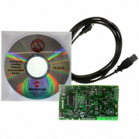
Manufacturer Part Number
TMPSNS-RTD1
Description
BOARD EVAL PT100 RTD TEMP SENSOR
Manufacturer
Microchip Technology
Datasheets
1.MCP3301-CIMS.pdf
(32 pages)
2.PCM18XR1.pdf
(438 pages)
3.MCP6S22DM-PICTL.pdf
(43 pages)
4.TMPSNS-RTD1.pdf
(26 pages)
Specifications of TMPSNS-RTD1
Sensor Type
Temperature
Interface
USB
Embedded
Yes, MCU, 8-Bit
Utilized Ic / Part
MCP3301, MCP6S26, PIC18F2550
Processor To Be Evaluated
MCP6S26, MCP3301, MCP6024, MCP41010, PIC18F2550, TC1071, MCP6002
Data Bus Width
12 bit
Interface Type
USB
Lead Free Status / RoHS Status
Not applicable / Not applicable
Voltage - Supply
-
Sensitivity
-
Sensing Range
-
Lead Free Status / RoHS Status
Lead free / RoHS Compliant, Not applicable / Not applicable


PIC18F2455/2550/4455/4550
17.2
The operation of the USB module is configured and
managed through three control registers. In addition, a
total of 22 registers are used to manage the actual USB
transactions. The registers are:
• USB Control register (UCON)
• USB Configuration register (UCFG)
• USB Transfer Status register (USTAT)
• USB Device Address register (UADDR)
• Frame Number registers (UFRMH:UFRML)
• Endpoint Enable registers 0 through 15 (UEPn)
17.2.1
The USB Control register (Register 17-1) contains bits
needed to control the module behavior during transfers.
The register contains bits that control the following:
• Main USB Peripheral Enable
• Ping-Pong Buffer Pointer Reset
• Control of the Suspend mode
• Packet Transfer Disable
REGISTER 17-1:
DS39632E-page 166
bit 7
Legend:
R = Readable bit
-n = Value at POR
bit 7
bit 6
bit 5
bit 4
bit 3
bit 2
bit 1
bit 0
U-0
—
USB Status and Control
USB CONTROL REGISTER (UCON)
Unimplemented: Read as ‘0’
PPBRST: Ping-Pong Buffers Reset bit
1 = Reset all Ping-Pong Buffer Pointers to the Even Buffer Descriptor (BD) banks
0 = Ping-Pong Buffer Pointers not being reset
SE0: Live Single-Ended Zero Flag bit
1 = Single-ended zero active on the USB bus
0 = No single-ended zero detected
PKTDIS: Packet Transfer Disable bit
1 = SIE token and packet processing disabled, automatically set when a SETUP token is received
0 = SIE token and packet processing enabled
USBEN: USB Module Enable bit
1 = USB module and supporting circuitry enabled (device attached)
0 = USB module and supporting circuitry disabled (device detached)
RESUME: Resume Signaling Enable bit
1 = Resume signaling activated
0 = Resume signaling disabled
SUSPND: Suspend USB bit
1 = USB module and supporting circuitry in Power Conserve mode, SIE clock inactive
0 = USB module and supporting circuitry in normal operation, SIE clock clocked at the configured rate
Unimplemented: Read as ‘0’
PPBRST
R/W-0
UCON: USB CONTROL REGISTER
C = Clearable bit
W = Writable bit
‘1’ = Bit is set
SE0
R-x
PKTDIS
R/C-0
U = Unimplemented bit, read as ‘0’
‘0’ = Bit is cleared
USBEN
R/W-0
In addition, the USB Control register contains a status bit,
SE0 (UCON<5>), which is used to indicate the occur-
rence of a single-ended zero on the bus. When the USB
module is enabled, this bit should be monitored to deter-
mine whether the differential data lines have come out of
a single-ended zero condition. This helps to differentiate
the initial power-up state from the USB Reset signal.
The overall operation of the USB module is controlled by
the USBEN bit (UCON<3>). Setting this bit activates the
module and resets all of the PPBI bits in the Buffer
Descriptor Table to ‘0’. This bit also activates the on-chip
voltage regulator (if the VREGEN Configuration bit is
set) and connects internal pull-up resistors, if they are
enabled. Thus, this bit can be used as a soft
attach/detach to the USB. Although all status and control
bits are ignored when this bit is clear, the module needs
to be fully preconfigured prior to setting this bit.
Note:
When disabling the USB module, make
sure the SUSPND bit (UCON<1>) is clear
prior to clearing the USBEN bit. Clearing
the USBEN bit when the module is in the
suspended state may prevent the module
from fully powering down.
RESUME
R/W-0
© 2009 Microchip Technology Inc.
x = Bit is unknown
SUSPND
R/W-0
U-0
—
bit 0
Related parts for TMPSNS-RTD1
Image
Part Number
Description
Manufacturer
Datasheet
Request
R

Part Number:
Description:
Manufacturer:
Microchip Technology Inc.
Datasheet:
Part Number:
Description:
Manufacturer:
Microchip Technology Inc.
Datasheet:
Part Number:
Description:
Manufacturer:
Microchip Technology Inc.
Datasheet:
Part Number:
Description:
Manufacturer:
Microchip Technology Inc.
Datasheet:
Part Number:
Description:
Manufacturer:
Microchip Technology Inc.
Datasheet:
Part Number:
Description:
Manufacturer:
Microchip Technology Inc.
Datasheet:
Part Number:
Description:
Manufacturer:
Microchip Technology Inc.
Datasheet:
Part Number:
Description:
Manufacturer:
Microchip Technology Inc.
Datasheet: