TMPSNS-RTD1 Microchip Technology, TMPSNS-RTD1 Datasheet - Page 406
TMPSNS-RTD1
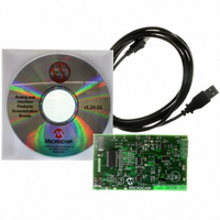
Manufacturer Part Number
TMPSNS-RTD1
Description
BOARD EVAL PT100 RTD TEMP SENSOR
Manufacturer
Microchip Technology
Datasheets
1.MCP3301-CIMS.pdf
(32 pages)
2.PCM18XR1.pdf
(438 pages)
3.MCP6S22DM-PICTL.pdf
(43 pages)
4.TMPSNS-RTD1.pdf
(26 pages)
Specifications of TMPSNS-RTD1
Sensor Type
Temperature
Interface
USB
Embedded
Yes, MCU, 8-Bit
Utilized Ic / Part
MCP3301, MCP6S26, PIC18F2550
Processor To Be Evaluated
MCP6S26, MCP3301, MCP6024, MCP41010, PIC18F2550, TC1071, MCP6002
Data Bus Width
12 bit
Interface Type
USB
Lead Free Status / RoHS Status
Not applicable / Not applicable
Voltage - Supply
-
Sensitivity
-
Sensing Range
-
Lead Free Status / RoHS Status
Lead free / RoHS Compliant, Not applicable / Not applicable


PIC18F2455/2550/4455/4550
TABLE 28-28: A/D CONVERTER CHARACTERISTICS: PIC18F2455/2550/4455/4550 (INDUSTRIAL)
FIGURE 28-23:
DS39632E-page 404
Param
A01
A03
A04
A06
A07
A10
A20
A21
A22
A25
A30
A50
Note 1:
No.
Note 1:
A/D DATA
2:
SAMPLE
A/D CLK
ADRES
Symbol
N
E
E
E
E
—
ΔV
V
V
V
Z
I
BSF ADCON0, GO
REF
REFH
REFL
AIN
AIN
IL
DL
OFF
GN
ADIF
R
REF
GO
The A/D conversion result never decreases with an increase in the input voltage and has no missing codes.
V
V
Q4
2:
REFH
REFL
If the A/D clock source is selected as RC, a time of T
This allows the SLEEP instruction to be executed.
This is a minimal RC delay (typically 100 ns), which also disconnects the holding capacitor from the analog input.
Resolution
Integral Linearity Error
Differential Linearity Error
Offset Error
Gain Error
Monotonicity
Reference Voltage Range
(V
Reference Voltage High
Reference Voltage Low
Analog Input Voltage
Recommended Impedance of
Analog Voltage Source
V
132
current is from RA2/AN2/V
current is from RA3/AN3/V
REF
REFH
A/D CONVERSION TIMING
Input Current
– V
Characteristic
REFL
(Note 2)
)
9
(2)
8
REF
REF
OLD_DATA
-/CV
+ pin or V
7
SAMPLING STOPPED
REF
ΔV
V
. . .
Vss +
Min
V
1.8
3.0
REFL
—
—
—
—
—
—
—
—
CY
REF
SS
pin or V
DD
is added before the A/D clock starts.
, whichever is selected as the V
. . .
131
130
Guaranteed
SS
PIC18LF2455/2550/4455/4550 (INDUSTRIAL)
Typ
, whichever is selected as the V
—
—
—
—
—
—
—
—
—
—
—
—
—
3
(1)
V
V
V
DD
2
DD
DD
V
<±2.0
Max
V
<±1
<±1
<±1
150
REFH
2.5
- ΔV
10
5
– V
– V
DD
REF
SS
SS
1
© 2009 Microchip Technology Inc.
Units
LSB ΔV
LSB ΔV
LSB ΔV
LSB ΔV
kΩ
μA
μA
bit
—
0
V
V
V
V
V
REFH
ΔV
V
V
V
During V
During A/D conversion
cycle.
NEW_DATA
DONE
SS
DD
DD
REF
REF
REF
REF
REF
source.
REFL
≤ V
< 3.0V
≥ 3.0V
Conditions
T
T
≥ 3.0V
≥ 3.0V
≥ 3.0V
≥ 3.0V
≥ 3.0V
CY
DIS
AIN
AIN
(1)
source.
≤ V
acquisition.
REF
Related parts for TMPSNS-RTD1
Image
Part Number
Description
Manufacturer
Datasheet
Request
R

Part Number:
Description:
Manufacturer:
Microchip Technology Inc.
Datasheet:
Part Number:
Description:
Manufacturer:
Microchip Technology Inc.
Datasheet:
Part Number:
Description:
Manufacturer:
Microchip Technology Inc.
Datasheet:
Part Number:
Description:
Manufacturer:
Microchip Technology Inc.
Datasheet:
Part Number:
Description:
Manufacturer:
Microchip Technology Inc.
Datasheet:
Part Number:
Description:
Manufacturer:
Microchip Technology Inc.
Datasheet:
Part Number:
Description:
Manufacturer:
Microchip Technology Inc.
Datasheet:
Part Number:
Description:
Manufacturer:
Microchip Technology Inc.
Datasheet: