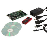
DV164136 Microchip Technology, DV164136 Datasheet - Page 100

DV164136
Manufacturer Part Number
DV164136
Description
DEVELOPMENT KIT FOR PIC18
Manufacturer
Microchip Technology
Series
PIC®r
Type
MCUr
Datasheets
1.DM183032.pdf
(38 pages)
2.DV164136.pdf
(448 pages)
3.DV164136.pdf
(6 pages)
4.DV164136.pdf
(446 pages)
5.DV164136.pdf
(4 pages)
6.DV164136.pdf
(18 pages)
Specifications of DV164136
Contents
Board, Cables, CDs, PICkit™ 3 Programmer, Power Supply
Processor To Be Evaluated
PIC18F8722, PIC18F87J11
Interface Type
RS-232, USB
Operating Supply Voltage
3.3 V, 5 V
Silicon Manufacturer
Microchip
Core Architecture
PIC
Core Sub-architecture
PIC18
Silicon Core Number
PIC18F
Silicon Family Name
PIC18F8xxx
Kit Contents
PIC18 Exp Brd PICkit 3 Cable CD PSU
Lead Free Status / RoHS Status
Lead free / RoHS Compliant
For Use With/related Products
PIC18F8722, PIC18F87J11
Lead Free Status / Rohs Status
Lead free / RoHS Compliant
Available stocks
Company
Part Number
Manufacturer
Quantity
Price
Company:
Part Number:
DV164136
Manufacturer:
MICROCHIP
Quantity:
12 000
- DM183032 PDF datasheet
- DV164136 PDF datasheet #2
- DV164136 PDF datasheet #3
- DV164136 PDF datasheet #4
- DV164136 PDF datasheet #5
- DV164136 PDF datasheet #6
- Current page: 100 of 448
- Download datasheet (8Mb)
PIC18F87J11 FAMILY
7.1
The operation of the interface is controlled by the
MEMCON register (Register 7-1). This register is
available in all program memory operating modes
except Microcontroller mode. In this mode, the register
is disabled and cannot be written to.
The EBDIS bit (MEMCON<7>) controls the operation
of the bus and related port functions. Clearing EBDIS
enables the interface and disables the I/O functions of
the ports, as well as any other functions multiplexed to
those pins. Setting the bit enables the I/O ports and
other functions, but allows the interface to override
everything else on the pins when an external memory
operation is required. By default, the external bus is
always enabled and disables all other I/O.
The operation of the EBDIS bit is also influenced by the
program memory mode being used. This is discussed
in more detail in Section 7.5 “Program Memory
Modes and the External Memory Bus”.
REGISTER 7-1:
DS39778D-page 100
bit 7
Legend:
R = Readable bit
-n = Value at POR
bit 7
bit 6
bit 5-4
bit 3-2
bit 1-0
EBDIS
R/W-0
External Memory Bus Control
EBDIS: External Bus Disable bit
1 = External bus enabled when microcontroller accesses external memory; otherwise, all external bus
0 = External bus always enabled, I/O ports are disabled
Unimplemented: Read as ‘0’
WAIT1:WAIT0: Table Reads and Writes Bus Cycle Wait Count bits
11 = Table reads and writes will wait 0 T
10 = Table reads and writes will wait 1 T
01 = Table reads and writes will wait 2 T
00 = Table reads and writes will wait 3 T
Unimplemented: Read as ‘0’
WM1:WM0: TBLWT Operation with 16-Bit Data Bus Width Select bits
1x = Word Write mode: TABLAT word output, WRH active when TABLAT written
01 = Byte Select mode: TABLAT data copied on both MSB and LSB, WRH and (UB or LB) will activate
00 = Byte Write mode: TABLAT data copied on both MSB and LSB, WRH or WRL will activate
drivers are mapped as I/O ports
U-0
—
MEMCON: EXTERNAL MEMORY BUS CONTROL REGISTER
W = Writable bit
‘1’ = Bit is set
WAIT1
R/W-0
WAIT0
R/W-0
CY
CY
CY
CY
U = Unimplemented bit, read as ‘0’
‘0’ = Bit is cleared
The WAIT bits allow for the addition of wait states to
external memory operations. The use of these bits is
discussed in Section 7.3 “Wait States”.
The WM bits select the particular operating mode used
when the bus is operating in 16-Bit Data Width mode.
These are discussed in more detail in Section 7.6
“16-Bit Data Width Modes”. These bits have no effect
when an 8-bit Data Width mode is selected.
The MEMCON register (see Register 7-1) shares the
same memory space as the PR2 register and can be
alternately selected based on the designation of the
ADSHR
Register 24-9).
U-0
—
bit
U-0
in
—
the
© 2009 Microchip Technology Inc.
x = Bit is unknown
WDTCON
R/W-0
WM1
register
R/W-0
WM0
bit 0
(see
Related parts for DV164136
Image
Part Number
Description
Manufacturer
Datasheet
Request
R

Part Number:
Description:
Manufacturer:
Microchip Technology Inc.
Datasheet:

Part Number:
Description:
Manufacturer:
Microchip Technology Inc.
Datasheet:

Part Number:
Description:
Manufacturer:
Microchip Technology Inc.
Datasheet:

Part Number:
Description:
Manufacturer:
Microchip Technology Inc.
Datasheet:

Part Number:
Description:
Manufacturer:
Microchip Technology Inc.
Datasheet:

Part Number:
Description:
Manufacturer:
Microchip Technology Inc.
Datasheet:

Part Number:
Description:
Manufacturer:
Microchip Technology Inc.
Datasheet:

Part Number:
Description:
Manufacturer:
Microchip Technology Inc.
Datasheet:


