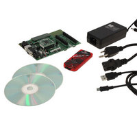
DV164136 Microchip Technology, DV164136 Datasheet - Page 163

DV164136
Manufacturer Part Number
DV164136
Description
DEVELOPMENT KIT FOR PIC18
Manufacturer
Microchip Technology
Series
PIC®r
Type
MCUr
Datasheets
1.DM183032.pdf
(38 pages)
2.DV164136.pdf
(448 pages)
3.DV164136.pdf
(6 pages)
4.DV164136.pdf
(446 pages)
5.DV164136.pdf
(4 pages)
6.DV164136.pdf
(18 pages)
Specifications of DV164136
Contents
Board, Cables, CDs, PICkit™ 3 Programmer, Power Supply
Processor To Be Evaluated
PIC18F8722, PIC18F87J11
Interface Type
RS-232, USB
Operating Supply Voltage
3.3 V, 5 V
Silicon Manufacturer
Microchip
Core Architecture
PIC
Core Sub-architecture
PIC18
Silicon Core Number
PIC18F
Silicon Family Name
PIC18F8xxx
Kit Contents
PIC18 Exp Brd PICkit 3 Cable CD PSU
Lead Free Status / RoHS Status
Lead free / RoHS Compliant
For Use With/related Products
PIC18F8722, PIC18F87J11
Lead Free Status / Rohs Status
Lead free / RoHS Compliant
Available stocks
Company
Part Number
Manufacturer
Quantity
Price
Company:
Part Number:
DV164136
Manufacturer:
MICROCHIP
Quantity:
12 000
- DM183032 PDF datasheet
- DV164136 PDF datasheet #2
- DV164136 PDF datasheet #3
- DV164136 PDF datasheet #4
- DV164136 PDF datasheet #5
- DV164136 PDF datasheet #6
- Current page: 163 of 448
- Download datasheet (8Mb)
11.2.2
Buffered Parallel Slave Port mode is functionally iden-
tical to the Legacy Parallel Slave Port mode with one
exception: the implementation of 4-level read and write
buffers. Buffered PSP mode is enabled by setting the
INCM bits in the PMMODE register. If the INCM<1:0>
bits are set to ‘11’, the PMP module will act as the
Buffered Parallel Slave Port.
When
PMDIN1L,PMDIN1H, PMDIN2L and PMDIN2H regis-
ters become the write buffers and the PMDOUT1L,
PMDOUT1H, PMDOUT2L and PMDOUT2H registers
become the read buffers. Buffers are numbered 0
through 3, starting with the lower byte of PMDIN1L to
PMDIN2H as the read buffers, and PMDOUT1L to
PMDOUT2H as the write buffers.
11.2.2.1
For read operations, the bytes will be sent out sequen-
tially, starting with Buffer 0 (PMDOUT1L<7:0>) and
ending with Buffer 3 (PMDOUT2H<7:0>) for every read
strobe. The module maintains an internal pointer to
keep track of which buffer is to be read. Each of the buf-
fers has a corresponding read status bit, OBxE, in the
PMSTATL register. This bit is cleared when a buffer
contains data that has not been written to the bus, and
is set when data is written to the bus. If the current buf-
fer location being read from is empty, a buffer underflow
FIGURE 11-5:
© 2009 Microchip Technology Inc.
Master
the
PMD<7:0>
BUFFERED PARALLEL SLAVE
PORT MODE
PMWR
PMRD
PMCS
READ FROM SLAVE PORT
Buffered
PARALLEL MASTER/SLAVE CONNECTION BUFFERED EXAMPLE
Data Bus
Control Lines
mode
is
active,
the
PMD<7:0>
PMCS1
PMRD
PMWR
PIC18F87J11 FAMILY
is generated, and the Buffer Overflow flag bit OBUF is
set. If all 4 OBxE status bits are set, then the Output
Buffer Empty flag (OBE) will also be set.
11.2.2.2
For write operations, the data is be stored sequentially,
starting with Buffer 0 (PMDIN1L<7:0>) and ending with
Buffer 3 (PMDIN2H<7:0). As with read operations, the
module maintains an internal pointer to the buffer that
is to be written next.
The input buffers have their own write status bits, IBxF
in the PMSTATH register. The bit is set when the buffer
contains unread incoming data, and cleared when the
data has been read. The flag bit is set on the write
strobe. If a write occurs on a buffer when its associated
IBxF bit is set, the Buffer Overflow flag, IBOV, is set;
any incoming data in the buffer will be lost. If all 4 IBxF
flags are set, the Input Buffer Full Flag (IBF) is set.
In Buffered Slave mode, the module can be configured
to generate an interrupt on every read or write strobe
(IRQM1:IRQM0 = 01). It can be configured to generate
an interrupt on a read from Read Buffer 3 or a write to
Write Buffer 3, which is essentially an interrupt every
fourth read or write strobe (RQM1:IRQM0 = 11). When
interrupting every fourth byte for input data, all input
buffer registers should be read to clear the IBxF flags.
If these flags are not cleared, then their is a risk of
hitting an overflow condition.
Address
Pointer
Write
PMDOUT1L (0)
PMDOUT1H (1)
PMDOUT2H (3)
PMDOUT2L (2)
PIC18 Slave
WRITE TO SLAVE PORT
Address
Pointer
Read
PMDIN1H (1)
PMDIN2H (3)
PMDIN1L (0)
PMDIN2L (2)
DS39778D-page 163
Related parts for DV164136
Image
Part Number
Description
Manufacturer
Datasheet
Request
R

Part Number:
Description:
Manufacturer:
Microchip Technology Inc.
Datasheet:

Part Number:
Description:
Manufacturer:
Microchip Technology Inc.
Datasheet:

Part Number:
Description:
Manufacturer:
Microchip Technology Inc.
Datasheet:

Part Number:
Description:
Manufacturer:
Microchip Technology Inc.
Datasheet:

Part Number:
Description:
Manufacturer:
Microchip Technology Inc.
Datasheet:

Part Number:
Description:
Manufacturer:
Microchip Technology Inc.
Datasheet:

Part Number:
Description:
Manufacturer:
Microchip Technology Inc.
Datasheet:

Part Number:
Description:
Manufacturer:
Microchip Technology Inc.
Datasheet:


