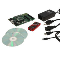
DV164136 Microchip Technology, DV164136 Datasheet - Page 130

DV164136
Manufacturer Part Number
DV164136
Description
DEVELOPMENT KIT FOR PIC18
Manufacturer
Microchip Technology
Series
PIC®r
Type
MCUr
Datasheets
1.DM183032.pdf
(38 pages)
2.DV164136.pdf
(448 pages)
3.DV164136.pdf
(6 pages)
4.DV164136.pdf
(446 pages)
5.DV164136.pdf
(4 pages)
6.DV164136.pdf
(18 pages)
Specifications of DV164136
Contents
Board, Cables, CDs, PICkit™ 3 Programmer, Power Supply
Processor To Be Evaluated
PIC18F8722, PIC18F87J11
Interface Type
RS-232, USB
Operating Supply Voltage
3.3 V, 5 V
Silicon Manufacturer
Microchip
Core Architecture
PIC
Core Sub-architecture
PIC18
Silicon Core Number
PIC18F
Silicon Family Name
PIC18F8xxx
Kit Contents
PIC18 Exp Brd PICkit 3 Cable CD PSU
Lead Free Status / RoHS Status
Lead free / RoHS Compliant
For Use With/related Products
PIC18F8722, PIC18F87J11
Lead Free Status / Rohs Status
Lead free / RoHS Compliant
Available stocks
Company
Part Number
Manufacturer
Quantity
Price
Company:
Part Number:
DV164136
Manufacturer:
MICROCHIP
Quantity:
12 000
- DM183032 PDF datasheet
- DV164136 PDF datasheet #2
- DV164136 PDF datasheet #3
- DV164136 PDF datasheet #4
- DV164136 PDF datasheet #5
- DV164136 PDF datasheet #6
- Current page: 130 of 448
- Download datasheet (8Mb)
PIC18F87J11 FAMILY
Table 10-2 summarizes the output capabilities of the
ports. Refer to the “Absolute Maximum Ratings” in
Section 27.0 “Electrical Characteristics” for more
details.
TABLE 10-2:
10.1.3
Four of the I/O ports (PORTB, PORTD, PORTE and
PORTJ) implement configurable weak pull-ups on all
pins. These are internal pull-ups that allow floating
digital input signals to be pulled to a consistent level,
without the use of external resistors.
The pull-ups are enabled with a single bit for each of the
ports: RBPU (INTCON2<7>) for PORTB, and RDPU,
REPU and RJPU (PORTG<7:5>) for the other ports.
10.1.4
The output pins for several peripherals are also
equipped with a configurable, open-drain output option.
This allows the peripherals to communicate with
external digital logic operating at a higher voltage level,
without the use of level translators.
The open-drain option is implemented on port pins spe-
cifically associated with the data and clock outputs of
the EUSARTs, the MSSP modules (in SPI mode) and
the CCP and ECCP modules. It is selectively enabled
by setting the open-drain control bit for the correspond-
ing module in the ODCON registers (Register 10-1,
Register 10-2 and Register 10-3). Their configuration
is discussed in more detail with the individual port
where these peripherals are multiplexed.
The ODCON registers all reside in the SFR configuration
space and share the same SFR addresses as the Timer1
registers (see Section 5.3.4.1 “Shared Address SFRs”
for more details). The ODCON registers are accessed by
setting the ADSHR bit (WDTCON<4>).
DS39778D-page 130
PORTA
PORTF
PORTG
PORTH
PORTD
PORTE
PORTJ
PORTB
PORTC
Note 1:
Port
(1)
(1)
These ports are not available on 64-pin
devices.
PULL-UP CONFIGURATION
OPEN-DRAIN OUTPUTS
Minimum Intended for indication.
Medium
Drive
High
OUTPUT DRIVE LEVELS
Sufficient drive levels for
external memory interfacing
as well as indication.
Suitable for direct LED drive
levels.
Description
When the open-drain option is required, the output pin
must also be tied through an external pull-up resistor
provided by the user to a higher voltage level, up to 5V
on digital only pins (Figure 10-2). When a digital logic
high signal is output, it is pulled up to the higher voltage
level.
FIGURE 10-2:
10.1.5
Many of the digital I/O ports use Schmitt Trigger (ST)
input buffers. While this form of buffering works well
with many types of input, some applications may
require TTL-level signals to interface with external logic
devices. This is particularly true with the EMB and the
Parallel Master Port (PMP), which are particularly likely
to be interfaced to TTL-level logic or memory devices.
The inputs for the PMP can be optionally configured for
TTL buffers with the PMPTTL bit in the PADCFG1 reg-
ister (Register 10-4). Setting this bit configures all data
and control input pins for the PMP to use TTL buffers.
By default, these PMP inputs use the port’s ST buffers.
As with the ODCON registers, the PADCFG1 register
resides in the SFR configuration space; it shares the
same memory address as the TMR2 register.
PADCFG1 is accessed by setting the ADSHR bit
(WDTCON<4>).
3.3V
TTL INPUT BUFFER OPTION
V
DD
PIC18F87J11
(at logic ‘1’)
USING THE OPEN-DRAIN
OUTPUT (EUSARTx
SHOWN AS EXAMPLE)
© 2009 Microchip Technology Inc.
TX
X
3.3V
+5V
5V
Related parts for DV164136
Image
Part Number
Description
Manufacturer
Datasheet
Request
R

Part Number:
Description:
Manufacturer:
Microchip Technology Inc.
Datasheet:

Part Number:
Description:
Manufacturer:
Microchip Technology Inc.
Datasheet:

Part Number:
Description:
Manufacturer:
Microchip Technology Inc.
Datasheet:

Part Number:
Description:
Manufacturer:
Microchip Technology Inc.
Datasheet:

Part Number:
Description:
Manufacturer:
Microchip Technology Inc.
Datasheet:

Part Number:
Description:
Manufacturer:
Microchip Technology Inc.
Datasheet:

Part Number:
Description:
Manufacturer:
Microchip Technology Inc.
Datasheet:

Part Number:
Description:
Manufacturer:
Microchip Technology Inc.
Datasheet:


