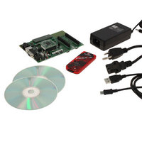
DV164136 Microchip Technology, DV164136 Datasheet - Page 307

DV164136
Manufacturer Part Number
DV164136
Description
DEVELOPMENT KIT FOR PIC18
Manufacturer
Microchip Technology
Series
PIC®r
Type
MCUr
Datasheets
1.DM183032.pdf
(38 pages)
2.DV164136.pdf
(448 pages)
3.DV164136.pdf
(6 pages)
4.DV164136.pdf
(446 pages)
5.DV164136.pdf
(4 pages)
6.DV164136.pdf
(18 pages)
Specifications of DV164136
Contents
Board, Cables, CDs, PICkit™ 3 Programmer, Power Supply
Processor To Be Evaluated
PIC18F8722, PIC18F87J11
Interface Type
RS-232, USB
Operating Supply Voltage
3.3 V, 5 V
Silicon Manufacturer
Microchip
Core Architecture
PIC
Core Sub-architecture
PIC18
Silicon Core Number
PIC18F
Silicon Family Name
PIC18F8xxx
Kit Contents
PIC18 Exp Brd PICkit 3 Cable CD PSU
Lead Free Status / RoHS Status
Lead free / RoHS Compliant
For Use With/related Products
PIC18F8722, PIC18F87J11
Lead Free Status / Rohs Status
Lead free / RoHS Compliant
Available stocks
Company
Part Number
Manufacturer
Quantity
Price
Company:
Part Number:
DV164136
Manufacturer:
MICROCHIP
Quantity:
12 000
- DM183032 PDF datasheet
- DV164136 PDF datasheet #2
- DV164136 PDF datasheet #3
- DV164136 PDF datasheet #4
- DV164136 PDF datasheet #5
- DV164136 PDF datasheet #6
- Current page: 307 of 448
- Download datasheet (8Mb)
22.5
Each comparator has up to eight possible combina-
tions of inputs: up to four external analog inputs, and
one of two internal voltage references.
Both comparators allow a selection of the signal from
pin, CxINA, or the voltage from the comparator refer-
ence (CV
compared to either CxINB, CxINC, CxIND or the micro-
controller’s fixed internal reference voltage (V
nominal) on the inverting channel. The comparator
inputs and outputs are tied to fixed I/O pins, defined in
Table 22-1. The available configurations and their
corresponding bit settings are shown in Figure 22-1.
TABLE 22-1:
22.5.1
Setting the CON bit of the CMxCON register
(CMxCON<7>) enables the comparator for operation.
Clearing the CON bit disables the comparator resulting
in minimum current consumption.
The CCH1:CCH0 bits in the CMxCON register
(CMxCON<1:0>) direct either one of three analog input
pins, or the Internal Reference Voltage (V
comparator V
ing mode, either an external or internal voltage
reference may be used. The analog signal present at
V
output of the comparator is adjusted accordingly.
The external reference is used when CREF = 0
(CMxCON<2>) and V
pin. When external voltage references are used, the
comparator module can be configured to have the ref-
erence sources externally. The reference signal must
be between V
pin of the comparator.
© 2009 Microchip Technology Inc.
Note 1:
IN
Comparator
- is compared to the signal at V
1
2
Comparator Control and
Configuration
REF
Available in 80-pin devices only.
COMPARATOR ENABLE AND
INPUT SELECTION
IN
) on the non-inverting channel. This is
SS
-. Depending on the comparator operat-
and V
COMPARATOR INPUTS AND
OUTPUTS
Input or Output
C1INC (V
C2INC(V
C2IND(V
C1INA (V
C1INB (V
C2INA(V
C2INB(V
IN
DD
C1OUT
C2OUT
+ is connected to the CxINA
, and can be applied to either
IN
IN
IN
IN
IN
IN
IN
-)
-)
-)
+)
+)
-)
-)
(1)
(1)
(1)
IN
+ and the digital
I/O Pin
IRV
RH6
RH4
RH5
RF6
RF5
RF2
RF4
RF3
RF1
IRV
), to the
(1)
(1)
(1)
, 1.2V
PIC18F87J11 FAMILY
The comparator module also allows the selection of an
internally generated voltage reference (CV
the comparator voltage reference module. This module
is described in more detail in Section 23.0 “Compara-
tor Voltage Reference Module”. The reference from
the Comparator Voltage Reference module is only
available when CREF = 1. In this mode, the internal
voltage reference is applied to the comparator’s V
pin.
22.5.1.1
In PIC18F87J11 family devices, the C and D input chan-
nels for both comparators are linked to pins in PORTH
and cannot be reassigned to alternate analog inputs.
Because of this, 64-pin devices offer a total of 4 different
configurations for each comparator. In contrast, 80-pin
devices offer a choice of 6 configurations for Comparator
1, and 8 configurations for Comparator 2. The configura-
tions shown in Figure 22-1 are footnoted to indicate
where they are not available.
22.5.2
The comparator outputs are read through the CMSTAT
register. The CMSTAT<0> reads the Comparator 1 out-
put and CMSTAT<1> reads the Comparator 2 output.
These bits are read-only.
The comparator outputs may also be directly output to
the RF1 and RF2 I/O pins by setting the COE bit
(CMxCON<6>). When enabled, multiplexors in the
output path of the pins switch to the output of the com-
parator. The TRISF<1:2> bits still function as the digital
output enable for the RF1 and RF2 pins while in this
mode.
By default, the comparator’s output is at logic high
whenever the voltage on V
The polarity of the comparator outputs can be inverted
using the CPOL bit (CMxCON<5>).
The uncertainty of each of the comparators is related to
the input offset voltage and the response time given in
the specifications, as discussed in Section 22.2
“Comparator Operation”.
Note:
The comparator input pin selected by
CCH1:CH0 must be configured as an input
by setting both the corresponding TRISF or
TRISH bit, and the corresponding PCFG bit
in the ANCON1 register.
COMPARATOR ENABLE AND
OUTPUT SELECTION
Comparator Configurations in 64-Pin
and 80-Pin Devices
IN
+ is greater than on V
DS39778D-page 307
REF
) from
IN
IN
+
-.
Related parts for DV164136
Image
Part Number
Description
Manufacturer
Datasheet
Request
R

Part Number:
Description:
Manufacturer:
Microchip Technology Inc.
Datasheet:

Part Number:
Description:
Manufacturer:
Microchip Technology Inc.
Datasheet:

Part Number:
Description:
Manufacturer:
Microchip Technology Inc.
Datasheet:

Part Number:
Description:
Manufacturer:
Microchip Technology Inc.
Datasheet:

Part Number:
Description:
Manufacturer:
Microchip Technology Inc.
Datasheet:

Part Number:
Description:
Manufacturer:
Microchip Technology Inc.
Datasheet:

Part Number:
Description:
Manufacturer:
Microchip Technology Inc.
Datasheet:

Part Number:
Description:
Manufacturer:
Microchip Technology Inc.
Datasheet:


