DV164136 Microchip Technology, DV164136 Datasheet - Page 34

DV164136
Manufacturer Part Number
DV164136
Description
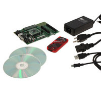
DEVELOPMENT KIT FOR PIC18
Manufacturer
Microchip Technology
Series
PIC®r
Type
MCUr
Datasheets
1.DM183032.pdf
(38 pages)
2.DV164136.pdf
(448 pages)
3.DV164136.pdf
(6 pages)
4.DV164136.pdf
(446 pages)
5.DV164136.pdf
(4 pages)
6.DV164136.pdf
(18 pages)
Specifications of DV164136
Contents
Board, Cables, CDs, PICkit™ 3 Programmer, Power Supply
Processor To Be Evaluated
PIC18F8722, PIC18F87J11
Interface Type
RS-232, USB
Operating Supply Voltage
3.3 V, 5 V
Silicon Manufacturer
Microchip
Core Architecture
PIC
Core Sub-architecture
PIC18
Silicon Core Number
PIC18F
Silicon Family Name
PIC18F8xxx
Kit Contents
PIC18 Exp Brd PICkit 3 Cable CD PSU
Lead Free Status / RoHS Status
Lead free / RoHS Compliant
For Use With/related Products
PIC18F8722, PIC18F87J11
Lead Free Status / Rohs Status
Lead free / RoHS Compliant
Available stocks
Company
Part Number
Manufacturer
Quantity
Price
Company:
Part Number:
DV164136
Manufacturer:
MICROCHIP
Quantity:
12 000
- DM183032 PDF datasheet
- DV164136 PDF datasheet #2
- DV164136 PDF datasheet #3
- DV164136 PDF datasheet #4
- DV164136 PDF datasheet #5
- DV164136 PDF datasheet #6
- Current page: 34 of 448
- Download datasheet (8Mb)
PIC18F87J11 FAMILY
2.2
The OSCCON register (Register 2-1) controls the main
aspects of the device clock’s operation. It selects the
oscillator type to be used, which of the power-managed
modes to invoke and the output frequency of the
INTOSC source. It also provides status on the oscillators.
REGISTER 2-1:
DS39778D-page 34
bit 7
Legend:
R = Readable bit
-n = Value at POR
bit 7
bit 6-4
bit 3
bit 2
bit 1-0
Note 1:
IDLEN
R/W-0
2:
3:
4:
5:
Control Registers
Default (legacy) SFR at this address, available when WDTCON<4> = 0.
Reset state depends on state of the IESO Configuration bit.
Modifying these bits will cause an immediate clock frequency switch if the internal oscillator is providing
the device clocks.
Source selected by the INTSRC bit (OSCTUNE<7>), see text.
Modifying these bits will cause an immediate clock source switch.
IDLEN: Idle Enable bit
1 = Device enters an Idle mode when a SLEEP instruction is executed
0 = Device enters Sleep mode when a SLEEP instruction is executed
IRCF2:IRCF0: INTOSC Source Frequency Select bits
111 = 8 MHz (INTOSC drives clock directly)
110 = 4 MHz (default)
101 = 2 MHz
100 = 1 MHz
011 = 500 kHz
010 = 250 kHz
001 = 125 kHz
000 = 31 kHz (from either INTOSC/256 or INTRC)
OSTS: Oscillator Start-up Timer Time-out Status bit
1 = Oscillator Start-up Timer (OST) time-out has expired; primary oscillator is running
0 = Oscillator Start-up Timer (OST) time-out is running; primary oscillator is not ready
Unimplemented: Read as ‘1’
SCS1:SCS0: System Clock Select bits
11 = Internal oscillator block
10 = Primary oscillator
01 = Timer1 oscillator
00 = Default primary oscillator (as defined by FOSC2:FOSC0 Configuration bits)
IRCF2
R/W-1
OSCCON: OSCILLATOR CONTROL REGISTER
(3)
W = Writable bit
‘1’ = Bit is set
IRCF1
R/W-1
(3)
IRCF0
R/W-0
(3)
(5)
U = Unimplemented bit, read as ‘0’
‘0’ = Bit is cleared
OSTS
The OSCTUNE register (Register 2-2) controls the
tuning and operation of the internal oscillator block. It
also implements the PLLEN bits which control the
operation of the Phase Locked Loop (PLL) (see
Section 2.4.3 “PLL Frequency Multiplier”).
R
(2)
(4)
(2)
(3)
(1)
U-1
—
© 2009 Microchip Technology Inc.
x = Bit is unknown
SCS1
R/W-0
(5)
SCS0
R/W-0
(5)
bit 0
Related parts for DV164136
Image
Part Number
Description
Manufacturer
Datasheet
Request
R

Part Number:
Description:
Manufacturer:
Microchip Technology Inc.
Datasheet:

Part Number:
Description:
Manufacturer:
Microchip Technology Inc.
Datasheet:

Part Number:
Description:
Manufacturer:
Microchip Technology Inc.
Datasheet:

Part Number:
Description:
Manufacturer:
Microchip Technology Inc.
Datasheet:

Part Number:
Description:
Manufacturer:
Microchip Technology Inc.
Datasheet:

Part Number:
Description:
Manufacturer:
Microchip Technology Inc.
Datasheet:

Part Number:
Description:
Manufacturer:
Microchip Technology Inc.
Datasheet:

Part Number:
Description:
Manufacturer:
Microchip Technology Inc.
Datasheet:


