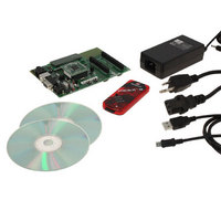
DV164136 Microchip Technology, DV164136 Datasheet - Page 161

DV164136
Manufacturer Part Number
DV164136
Description
DEVELOPMENT KIT FOR PIC18
Manufacturer
Microchip Technology
Series
PIC®r
Type
MCUr
Datasheets
1.DM183032.pdf
(38 pages)
2.DV164136.pdf
(448 pages)
3.DV164136.pdf
(6 pages)
4.DV164136.pdf
(446 pages)
5.DV164136.pdf
(4 pages)
6.DV164136.pdf
(18 pages)
Specifications of DV164136
Contents
Board, Cables, CDs, PICkit™ 3 Programmer, Power Supply
Processor To Be Evaluated
PIC18F8722, PIC18F87J11
Interface Type
RS-232, USB
Operating Supply Voltage
3.3 V, 5 V
Silicon Manufacturer
Microchip
Core Architecture
PIC
Core Sub-architecture
PIC18
Silicon Core Number
PIC18F
Silicon Family Name
PIC18F8xxx
Kit Contents
PIC18 Exp Brd PICkit 3 Cable CD PSU
Lead Free Status / RoHS Status
Lead free / RoHS Compliant
For Use With/related Products
PIC18F8722, PIC18F87J11
Lead Free Status / Rohs Status
Lead free / RoHS Compliant
Available stocks
Company
Part Number
Manufacturer
Quantity
Price
Company:
Part Number:
DV164136
Manufacturer:
MICROCHIP
Quantity:
12 000
- DM183032 PDF datasheet
- DV164136 PDF datasheet #2
- DV164136 PDF datasheet #3
- DV164136 PDF datasheet #4
- DV164136 PDF datasheet #5
- DV164136 PDF datasheet #6
- Current page: 161 of 448
- Download datasheet (8Mb)
11.1.4
By default, the PMP and the external memory bus
multiplex some of their signals to the same I/O pins on
PORTD and PORTE. It is possible that some applica-
tions may require the PMP signals to be located
elsewhere. For these instances, the 80-pin devices can
be configured to multiplex the PMP to different I/O
ports. PMP configuration is determined by the PMPMX
Configuration bit setting; by default, the PMP and EMB
modules share PORTD and PORTE. The optional pin
configuration is shown in Table 11-1.
TABLE 11-1:
FIGURE 11-2:
© 2009 Microchip Technology Inc.
PMP Function
PMWR
PMRD
PMD0
PMD1
PMD2
PMD3
PMD4
PMD5
PMD6
PMD7
PMBE
PMP MULTIPLEXING OPTIONS
(80-PIN DEVICES)
Master
PMD<7:0>
PMP PIN MULTIPLEXING FOR
80-PIN DEVICES
PMWR
PMRD
PMCS
PMPMX = 1
PORTD<0>
PORTD<1>
PORTD<2>
PORTD<3>
PORTD<4>
PORTD<5>
PORTD<6>
PORTD<7>
PORTE<2>
PORTE<1>
PORTE<0>
LEGACY PARALLEL SLAVE PORT EXAMPLE
Pin Assignment
PMPMX = 0
PORTH<4>
PORTH<3>
PORTH<2>
PORTH<5>
PORTH<7>
PORTH<6>
PORTF<7>
PORTF<6>
PORTF<5>
PORTA<5>
PORTA<4>
PMD<7:0>
PMCS1
PMRD
PMWR
PIC18F87J11 FAMILY
11.2
The primary mode of operation for the module is con-
figured using the MODE1:MODE0 bits in the
PMMODEH register. The setting affects whether the
module acts as a slave or a master and it determines
the usage of the control pins.
11.2.1
In
PMPEN = 1), the module is configured as a Parallel
Slave Port with the associated enabled module pins
dedicated to the module. In this mode, an external
device, such as another microcontroller or micropro-
cessor, can asynchronously read and write data using
the 8-bit data bus (PMD<7:0>), the read (PMRD), write
(PMWR) and chip select (PMCS1) inputs. It acts as a
slave on the bus and responds to the read/write control
signals.
Figure 11-2 shows the connection of the Parallel Slave
Port. When chip select is active and a write strobe
occurs (PMCS = 1 and PMWR = 1), the data from
PMD<7:0> is captured into the PMDIN1L register.
PIC18 Slave
Legacy
Slave Port Modes
LEGACY MODE (PSP)
mode
Address Bus
Data Bus
Control Lines
(PMMODEH<1:0> = 00
DS39778D-page 161
and
Related parts for DV164136
Image
Part Number
Description
Manufacturer
Datasheet
Request
R

Part Number:
Description:
Manufacturer:
Microchip Technology Inc.
Datasheet:

Part Number:
Description:
Manufacturer:
Microchip Technology Inc.
Datasheet:

Part Number:
Description:
Manufacturer:
Microchip Technology Inc.
Datasheet:

Part Number:
Description:
Manufacturer:
Microchip Technology Inc.
Datasheet:

Part Number:
Description:
Manufacturer:
Microchip Technology Inc.
Datasheet:

Part Number:
Description:
Manufacturer:
Microchip Technology Inc.
Datasheet:

Part Number:
Description:
Manufacturer:
Microchip Technology Inc.
Datasheet:

Part Number:
Description:
Manufacturer:
Microchip Technology Inc.
Datasheet:


