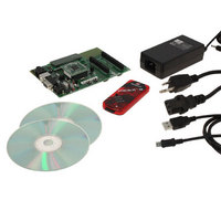
DV164136 Microchip Technology, DV164136 Datasheet - Page 148

DV164136
Manufacturer Part Number
DV164136
Description
DEVELOPMENT KIT FOR PIC18
Manufacturer
Microchip Technology
Series
PIC®r
Type
MCUr
Datasheets
1.DM183032.pdf
(38 pages)
2.DV164136.pdf
(448 pages)
3.DV164136.pdf
(6 pages)
4.DV164136.pdf
(446 pages)
5.DV164136.pdf
(4 pages)
6.DV164136.pdf
(18 pages)
Specifications of DV164136
Contents
Board, Cables, CDs, PICkit™ 3 Programmer, Power Supply
Processor To Be Evaluated
PIC18F8722, PIC18F87J11
Interface Type
RS-232, USB
Operating Supply Voltage
3.3 V, 5 V
Silicon Manufacturer
Microchip
Core Architecture
PIC
Core Sub-architecture
PIC18
Silicon Core Number
PIC18F
Silicon Family Name
PIC18F8xxx
Kit Contents
PIC18 Exp Brd PICkit 3 Cable CD PSU
Lead Free Status / RoHS Status
Lead free / RoHS Compliant
For Use With/related Products
PIC18F8722, PIC18F87J11
Lead Free Status / Rohs Status
Lead free / RoHS Compliant
Available stocks
Company
Part Number
Manufacturer
Quantity
Price
Company:
Part Number:
DV164136
Manufacturer:
MICROCHIP
Quantity:
12 000
- DM183032 PDF datasheet
- DV164136 PDF datasheet #2
- DV164136 PDF datasheet #3
- DV164136 PDF datasheet #4
- DV164136 PDF datasheet #5
- DV164136 PDF datasheet #6
- Current page: 148 of 448
- Download datasheet (8Mb)
PIC18F87J11 FAMILY
TABLE 10-17: SUMMARY OF REGISTERS ASSOCIATED WITH PORTG
10.9
PORTH is an 8-bit wide, bidirectional I/O port. PORTH
pins <3:0> are digital only and tolerate voltages up to
5.5V.
All pins on PORTH are implemented with Schmitt
Trigger input buffers. Each pin is individually
configurable as an input or output.
When the external memory interface is enabled, four of
the PORTH pins function as the high-order address
lines for the interface. The address output from the
interface takes priority over other digital I/O. The
corresponding TRISH bits are also overridden. PORTH
pins, RH4 through RH7, are multiplexed with analog
converter inputs. The operation of these pins as analog
inputs is selected by clearing or setting the
corresponding bits in the ANCON1 register. RH2 to
RH6 are multiplexed with the Parallel Master Port and
RH4 to RH6 are multiplexed as comparator inputs.
DS39778D-page 148
PORTG
LATG
TRISG
Legend: — = unimplemented, read as ‘0’. Shaded cells are not used by PORTG.
Note 1:
Note:
Name
PORTH, LATH and
TRISH Registers
PORTH is available only on 80-pin
devices.
Unimplemented on 64-pin devices, read as ‘0’.
RDPU
Bit 7
—
—
REPU
Bit 6
—
—
RJPU
Bit 5
—
—
(1)
TRISG4
LATG4
Bit 4
RG4
TRISG3
LATG3
PORTH can also be configured as the alternate
Enhanced PWM output channels B and C for the
ECCP1 and ECCP3 modules. This is done by clearing
the ECCPMX Configuration bit.
EXAMPLE 10-8:
Bit 3
CLRF
CLRF
BSF
MOVLW F0h
MOVWF ANCON1
BCF
MOVLW 0CFh
MOVWF TRISH
RG3
PORTH
LATH
WDTCON,ADSHR ; Enable write/read to
WDTCON,ADSHR ; Disable write/read to
TRISG2
LATG2
Bit 2
RG2
TRISG1
LATG1
INITIALIZING PORTH
Bit 1
RG1
; Initialize PORTH by
; clearing output
; data latches
; Alternate method to
; clear output latches
; the shared SFR
; Configure PORTH as
; digital I/O
; the shared SFR
; Value used to initialize
; data direction
; Set RH<3:0> as inputs
; RH<5:4> as outputs
; RH<7:6> as inputs
© 2009 Microchip Technology Inc.
TRISG0
LATG0
Bit 0
RG0
Values on
Reset
Page:
61
60
60
Related parts for DV164136
Image
Part Number
Description
Manufacturer
Datasheet
Request
R

Part Number:
Description:
Manufacturer:
Microchip Technology Inc.
Datasheet:

Part Number:
Description:
Manufacturer:
Microchip Technology Inc.
Datasheet:

Part Number:
Description:
Manufacturer:
Microchip Technology Inc.
Datasheet:

Part Number:
Description:
Manufacturer:
Microchip Technology Inc.
Datasheet:

Part Number:
Description:
Manufacturer:
Microchip Technology Inc.
Datasheet:

Part Number:
Description:
Manufacturer:
Microchip Technology Inc.
Datasheet:

Part Number:
Description:
Manufacturer:
Microchip Technology Inc.
Datasheet:

Part Number:
Description:
Manufacturer:
Microchip Technology Inc.
Datasheet:


