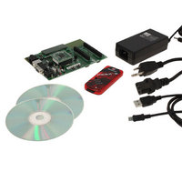
DV164136 Microchip Technology, DV164136 Datasheet - Page 76

DV164136
Manufacturer Part Number
DV164136
Description
DEVELOPMENT KIT FOR PIC18
Manufacturer
Microchip Technology
Series
PIC®r
Type
MCUr
Datasheets
1.DM183032.pdf
(38 pages)
2.DV164136.pdf
(448 pages)
3.DV164136.pdf
(6 pages)
4.DV164136.pdf
(446 pages)
5.DV164136.pdf
(4 pages)
6.DV164136.pdf
(18 pages)
Specifications of DV164136
Contents
Board, Cables, CDs, PICkit™ 3 Programmer, Power Supply
Processor To Be Evaluated
PIC18F8722, PIC18F87J11
Interface Type
RS-232, USB
Operating Supply Voltage
3.3 V, 5 V
Silicon Manufacturer
Microchip
Core Architecture
PIC
Core Sub-architecture
PIC18
Silicon Core Number
PIC18F
Silicon Family Name
PIC18F8xxx
Kit Contents
PIC18 Exp Brd PICkit 3 Cable CD PSU
Lead Free Status / RoHS Status
Lead free / RoHS Compliant
For Use With/related Products
PIC18F8722, PIC18F87J11
Lead Free Status / Rohs Status
Lead free / RoHS Compliant
Available stocks
Company
Part Number
Manufacturer
Quantity
Price
Company:
Part Number:
DV164136
Manufacturer:
MICROCHIP
Quantity:
12 000
- DM183032 PDF datasheet
- DV164136 PDF datasheet #2
- DV164136 PDF datasheet #3
- DV164136 PDF datasheet #4
- DV164136 PDF datasheet #5
- DV164136 PDF datasheet #6
- Current page: 76 of 448
- Download datasheet (8Mb)
PIC18F87J11 FAMILY
5.3.4.1
In several locations in the SFR bank, a single address
is used to access two different hardware registers. In
these cases, a “legacy” register of the standard PIC18
SFR set (such as OSCCON, T1CON, etc.) shares its
address with an alternate register. These alternate reg-
isters are associated with enhanced configuration
options for peripherals, or with new device features not
included in the standard PIC18 SFR map. A complete
list of shared register addresses and the registers
associated with them is provided in Table 5-4.
Access to the alternate registers is enabled in software
by setting the ADSHR bit in the WDTCON register
(Register 5-3). ADSHR must be manually set or
cleared to access the alternate or legacy registers, as
required. Since the bit remains in a given state until
changed, users should always verify the state of
ADSHR before writing to any of the shared SFR
addresses.
TABLE 5-4:
REGISTER 5-3:
DS39778D-page 76
Legend:
Note 1:
bit 7
Legend:
R = Readable bit
-n = Value at POR
bit 7
bit 6
bit 5
bit 4
bit 3-1
bit 0
REGSLP
FCFh
FCEh
FD3h
Address
R/W-0
(D) = Default SFR, accessible only when ADSHR = 0; (A) = Alternate SFR, accessible only when ADSHR = 1.
Implemented in 80-pin devices only.
(D)
(A)
(D)
(A)
(D)
(A)
Shared Address SFRs
REGSLP: Voltage Regulator Low-Power Operation Enable bit
For details of bit operation, see Register 24-9.
LVDSTAT: LVD Status bit
1 = V
0 = V
Unimplemented: Read as ‘0’
ADSHR: Shared Address SFR Select bit
1 = Alternate SFR is selected
0 = Default (Legacy) SFR is selected
Unimplemented: Read as ‘0’
SWDTEN: Software Controlled Watchdog Timer Enable bit
For details of bit operation, see Register 24-9.
LVDSTAT
SHARED SFR ADDRESSES FOR PIC18F87J11 FAMILY DEVICES
REFOCON
R-x
OSCCON
ODCON1
ODCON2
DDCORE
DDCORE
TMR1H
TMR1L
Name
WDTCON: WATCHDOG TIMER CONTROL REGISTER
> 2.45V
< 2.45V
W = Writable bit
‘1’ = Bit is set
U-0
—
FCDh
FCCh
FCBh
Address
ADSHR
R/W-0
(D)
(A)
(D)
(A)
(D)
(A)
U = Unimplemented bit, read as ‘0’
‘0’ = Bit is cleared
MEMCON
PADCFG1
ODCON3
5.3.4.2
In addition to the shared address SFRs, there are
several registers that share the same address in the
SFR space, but are not accessed with the ADSHR bit.
Instead, the register’s definition and use depends on
the operating mode of its associated peripheral. These
registers are:
• SSPxADD and SSPxMSK: These are two
• PMADDRH/L and PMDOUT2H/L: In this case,
T1CON
Name
TMR2
U-0
PR2
—
separate hardware registers, accessed through a
single SFR address. The operating mode of the
MSSP module determines which register is being
accessed. See Section 19.4.3.4 “7-Bit Address
Masking Mode” for additional details.
these named buffer pairs are actually the same
physical registers. The PMP module’s operating
mode determines what function the registers take
on. See Section 11.1.2 “Data Registers” for
additional details.
(1)
Context Defined SFRs
U-0
—
FC2h
FC1h
F77h
© 2009 Microchip Technology Inc.
Address
x = Bit is unknown
U-0
—
(D)
(A)
(D)
(D)
(A)
(A)
CVRCON
ADCON0
ANCON1
ADCON1
ANCON0
SWDTEN
Name
PR4
U-0
bit 0
Related parts for DV164136
Image
Part Number
Description
Manufacturer
Datasheet
Request
R

Part Number:
Description:
Manufacturer:
Microchip Technology Inc.
Datasheet:

Part Number:
Description:
Manufacturer:
Microchip Technology Inc.
Datasheet:

Part Number:
Description:
Manufacturer:
Microchip Technology Inc.
Datasheet:

Part Number:
Description:
Manufacturer:
Microchip Technology Inc.
Datasheet:

Part Number:
Description:
Manufacturer:
Microchip Technology Inc.
Datasheet:

Part Number:
Description:
Manufacturer:
Microchip Technology Inc.
Datasheet:

Part Number:
Description:
Manufacturer:
Microchip Technology Inc.
Datasheet:

Part Number:
Description:
Manufacturer:
Microchip Technology Inc.
Datasheet:


