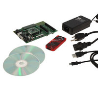
DV164136 Microchip Technology, DV164136 Datasheet - Page 46

DV164136
Manufacturer Part Number
DV164136
Description
DEVELOPMENT KIT FOR PIC18
Manufacturer
Microchip Technology
Series
PIC®r
Type
MCUr
Datasheets
1.DM183032.pdf
(38 pages)
2.DV164136.pdf
(448 pages)
3.DV164136.pdf
(6 pages)
4.DV164136.pdf
(446 pages)
5.DV164136.pdf
(4 pages)
6.DV164136.pdf
(18 pages)
Specifications of DV164136
Contents
Board, Cables, CDs, PICkit™ 3 Programmer, Power Supply
Processor To Be Evaluated
PIC18F8722, PIC18F87J11
Interface Type
RS-232, USB
Operating Supply Voltage
3.3 V, 5 V
Silicon Manufacturer
Microchip
Core Architecture
PIC
Core Sub-architecture
PIC18
Silicon Core Number
PIC18F
Silicon Family Name
PIC18F8xxx
Kit Contents
PIC18 Exp Brd PICkit 3 Cable CD PSU
Lead Free Status / RoHS Status
Lead free / RoHS Compliant
For Use With/related Products
PIC18F8722, PIC18F87J11
Lead Free Status / Rohs Status
Lead free / RoHS Compliant
Available stocks
Company
Part Number
Manufacturer
Quantity
Price
Company:
Part Number:
DV164136
Manufacturer:
MICROCHIP
Quantity:
12 000
- DM183032 PDF datasheet
- DV164136 PDF datasheet #2
- DV164136 PDF datasheet #3
- DV164136 PDF datasheet #4
- DV164136 PDF datasheet #5
- DV164136 PDF datasheet #6
- Current page: 46 of 448
- Download datasheet (8Mb)
PIC18F87J11 FAMILY
3.2.3
In RC_RUN mode, the CPU and peripherals are
clocked from the internal oscillator; the primary clock is
shut down. This mode provides the best power conser-
vation of all the Run modes while still executing code.
It works well for user applications which are not highly
timing sensitive or do not require high-speed clocks at
all times.
This mode is entered by setting SCS<1:0> to ‘11’.
When the clock source is switched to the internal
oscillator block (see Figure 3-3), the primary oscillator
is shut down and the OSTS bit is cleared.
FIGURE 3-3:
FIGURE 3-4:
DS39778D-page 46
Peripheral
Program
Counter
INTRC
OSC1
Note 1: T
Clock
Clock
RC_RUN MODE
CPU Clock
CPU
PLL Clock
Peripheral
Program
Counter
INTRC
Output
OSC1
Clock
Q1
OST
SCS1:SCS0 Bits Changed
Q2
= 1024 T
TRANSITION TIMING TO RC_RUN MODE
TRANSITION TIMING FROM RC_RUN MODE TO PRI_RUN MODE
PC
Q3
Q4
OSC
; T
Q1
Q1
PLL
T
1
= 2 ms (approx). These intervals are not shown to scale.
OST (1)
PC
Q2
2
Clock Transition
3
T
OSTS Bit Set
PLL
Q3
(1)
PC + 2
Q4
n-1
On transitions from RC_RUN mode to PRI_RUN mode,
the device continues to be clocked from the INTOSC
block while the primary clock is started. When the
primary clock becomes ready, a clock switch to the pri-
mary clock occurs (see Figure 3-4). When the clock
switch is complete, the OSTS bit is set and the primary
clock is providing the device clock. The IDLEN and
SCS bits are not affected by the switch. The INTRC
block source will continue to run if either the WDT or the
Fail-Safe Clock Monitor is enabled.
n
Q1
1
Transition
2
Clock
n-1 n
Q2
PC + 2
Q3
Q2
Q4
© 2009 Microchip Technology Inc.
Q3 Q4
Q1
Q1
PC + 4
Q2
Q2
PC + 4
Q3
Q3
Related parts for DV164136
Image
Part Number
Description
Manufacturer
Datasheet
Request
R

Part Number:
Description:
Manufacturer:
Microchip Technology Inc.
Datasheet:

Part Number:
Description:
Manufacturer:
Microchip Technology Inc.
Datasheet:

Part Number:
Description:
Manufacturer:
Microchip Technology Inc.
Datasheet:

Part Number:
Description:
Manufacturer:
Microchip Technology Inc.
Datasheet:

Part Number:
Description:
Manufacturer:
Microchip Technology Inc.
Datasheet:

Part Number:
Description:
Manufacturer:
Microchip Technology Inc.
Datasheet:

Part Number:
Description:
Manufacturer:
Microchip Technology Inc.
Datasheet:

Part Number:
Description:
Manufacturer:
Microchip Technology Inc.
Datasheet:


