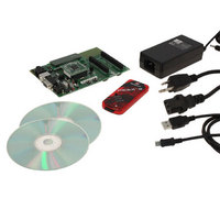
DV164136 Microchip Technology, DV164136 Datasheet - Page 35

DV164136
Manufacturer Part Number
DV164136
Description
DEVELOPMENT KIT FOR PIC18
Manufacturer
Microchip Technology
Series
PIC®r
Type
MCUr
Datasheets
1.DM183032.pdf
(38 pages)
2.DV164136.pdf
(448 pages)
3.DV164136.pdf
(6 pages)
4.DV164136.pdf
(446 pages)
5.DV164136.pdf
(4 pages)
6.DV164136.pdf
(18 pages)
Specifications of DV164136
Contents
Board, Cables, CDs, PICkit™ 3 Programmer, Power Supply
Processor To Be Evaluated
PIC18F8722, PIC18F87J11
Interface Type
RS-232, USB
Operating Supply Voltage
3.3 V, 5 V
Silicon Manufacturer
Microchip
Core Architecture
PIC
Core Sub-architecture
PIC18
Silicon Core Number
PIC18F
Silicon Family Name
PIC18F8xxx
Kit Contents
PIC18 Exp Brd PICkit 3 Cable CD PSU
Lead Free Status / RoHS Status
Lead free / RoHS Compliant
For Use With/related Products
PIC18F8722, PIC18F87J11
Lead Free Status / Rohs Status
Lead free / RoHS Compliant
Available stocks
Company
Part Number
Manufacturer
Quantity
Price
Company:
Part Number:
DV164136
Manufacturer:
MICROCHIP
Quantity:
12 000
- DM183032 PDF datasheet
- DV164136 PDF datasheet #2
- DV164136 PDF datasheet #3
- DV164136 PDF datasheet #4
- DV164136 PDF datasheet #5
- DV164136 PDF datasheet #6
- Current page: 35 of 448
- Download datasheet (8Mb)
REGISTER 2-2:
2.3
Essentially, PIC18F87J11 Family devices have three
independent clock sources:
• Primary oscillators
• Secondary oscillators
• Internal oscillator
The primary oscillators can be thought of as the main
device oscillators. These are any external oscillators
connected to the OSC1 and OSC2 pins, and include
the External Crystal and Resonator modes and the
External
FOSC2:FOSC0
oscillator block (either the 31 kHz INTRC or the 8 MHz
INTOSC source) may be considered a primary
oscillator. The particular mode is defined by the FOSC
Configuration bits. The details of these modes are
covered in Section 2.4 “External Oscillator Modes”.
The secondary oscillators are external clock sources
that are not connected to the OSC1 or OSC2 pins.
These sources may continue to operate even after the
controller is placed in a power-managed mode.
PIC18F87J11 Family devices offer the Timer1 oscillator
as a secondary oscillator source. This oscillator, in all
power-managed modes, is often the time base for
© 2009 Microchip Technology Inc.
bit 7
Legend:
R = Readable bit
-n = Value at POR
bit 7
bit 6
bit 5-0
INTSRC
R/W-0
Clock Sources and
Oscillator Switching
Clock
INTSRC: Internal Oscillator Low-Frequency Source Select bit
1 = 31.25 kHz device clock derived from 8 MHz INTOSC source (divide-by-256 enabled)
0 = 31 kHz device clock derived from INTRC 31 kHz oscillator
PLLEN: Frequency Multiplier PLL Enable bit
1 = PLL enabled
0 = PLL disabled
TUN5:TUN0: Fast RC Oscillator (INTOSC) Frequency Tuning bits
011111 = Maximum frequency
•
•
000001
000000 = Center frequency. Fast RC oscillator is running at the calibrated frequency.
111111
•
•
100000 = Minimum frequency
Configuration
PLLEN
R/W-0
modes.
OSCTUNE: OSCILLATOR TUNING REGISTER
W = Writable bit
‘1’ = Bit is set
If
R/W-0
TUN5
•
•
•
•
selected
bits,
the
by
internal
R/W-0
TUN4
the
U = Unimplemented bit, read as ‘0’
‘0’ = Bit is cleared
PIC18F87J11 FAMILY
R/W-0
TUN3
functions such as a Real-Time Clock (RTC). The
Timer1 oscillator is discussed in greater detail in
Section 13.0 “Timer1 Module”
In addition to being a primary clock source in some cir-
cumstances, the internal oscillator is available as a
power-managed mode clock source. The INTRC
source is also used as the clock source for several
special features, such as the WDT and Fail-Safe Clock
Monitor. The internal oscillator block is discussed in
more detail in Section 2.5 “Internal Oscillator
Block”.
The PIC18F87J11 Family includes features that allow
the device clock source to be switched from the main
oscillator, chosen by device configuration, to one of the
alternate clock sources. When an alternate clock
source is enabled, various power-managed operating
modes are available.
R/W-0
TUN2
x = Bit is unknown
R/W-0
TUN1
DS39778D-page 35
R/W-0
TUN0
bit 0
Related parts for DV164136
Image
Part Number
Description
Manufacturer
Datasheet
Request
R

Part Number:
Description:
Manufacturer:
Microchip Technology Inc.
Datasheet:

Part Number:
Description:
Manufacturer:
Microchip Technology Inc.
Datasheet:

Part Number:
Description:
Manufacturer:
Microchip Technology Inc.
Datasheet:

Part Number:
Description:
Manufacturer:
Microchip Technology Inc.
Datasheet:

Part Number:
Description:
Manufacturer:
Microchip Technology Inc.
Datasheet:

Part Number:
Description:
Manufacturer:
Microchip Technology Inc.
Datasheet:

Part Number:
Description:
Manufacturer:
Microchip Technology Inc.
Datasheet:

Part Number:
Description:
Manufacturer:
Microchip Technology Inc.
Datasheet:


