DEMO9S08EL32 Freescale Semiconductor, DEMO9S08EL32 Datasheet - Page 124
DEMO9S08EL32
Manufacturer Part Number
DEMO9S08EL32
Description
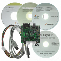
BOARD DEMO FOR 9S08 EL MCU
Manufacturer
Freescale Semiconductor
Type
MCUr
Datasheets
1.DEMO9S08EL32.pdf
(356 pages)
2.DEMO9S08EL32.pdf
(14 pages)
3.DEMO9S08EL32.pdf
(2 pages)
Specifications of DEMO9S08EL32
Contents
Evaluation Board
Processor To Be Evaluated
MC9S08EL32
Data Bus Width
8 bit
Interface Type
RS-232, USB
Operating Supply Voltage
12 V
Silicon Manufacturer
Freescale
Core Architecture
HCS08
Core Sub-architecture
HCS08
Silicon Core Number
MC9S08
Silicon Family Name
S08EL
Rohs Compliant
Yes
For Use With/related Products
MC9S08EL32
Lead Free Status / RoHS Status
Lead free / RoHS Compliant


Internal Clock Source (S08ICSV2)
In FLL engaged internal mode, the ICSOUT clock is derived from the FLL clock, which is controlled by
the internal reference clock. The FLL loop will lock the frequency to 1024 times the reference frequency,
as selected by the RDIV bits. The ICSLCLK is available for BDC communications, and the internal
reference clock is enabled.
8.4.1.2
The FLL engaged external (FEE) mode is entered when all the following conditions occur:
In FLL engaged external mode, the ICSOUT clock is derived from the FLL clock which is controlled by
the external reference clock.The FLL loop will lock the frequency to 1024 times the reference frequency,
as selected by the RDIV bits. The ICSLCLK is available for BDC communications, and the external
reference clock is enabled.
8.4.1.3
The FLL bypassed internal (FBI) mode is entered when all the following conditions occur:
In FLL bypassed internal mode, the ICSOUT clock is derived from the internal reference clock. The FLL
clock is controlled by the internal reference clock, and the FLL loop will lock the FLL frequency to 1024
times the reference frequency, as selected by the RDIV bits. The ICSLCLK will be available for BDC
communications, and the internal reference clock is enabled.
8.4.1.4
The FLL bypassed internal low power (FBILP) mode is entered when all the following conditions occur:
In FLL bypassed internal low power mode, the ICSOUT clock is derived from the internal reference clock
and the FLL is disabled. The ICSLCLK will be not be available for BDC communications, and the internal
reference clock is enabled.
124
•
•
•
•
•
•
•
•
•
•
•
•
CLKS bits are written to 00
IREFS bit is written to 1
RDIV bits are written to divide trimmed reference clock to be within the range of 31.25 kHz to
39.0625 kHz.
CLKS bits are written to 00
IREFS bit is written to 0
RDIV bits are written to divide reference clock to be within the range of 31.25 kHz to 39.0625 kHz
CLKS bits are written to 01
IREFS bit is written to 1.
BDM mode is active or LP bit is written to 0
CLKS bits are written to 01
IREFS bit is written to 1.
BDM mode is not active and LP bit is written to 1
FLL Engaged External (FEE)
FLL Bypassed Internal (FBI)
FLL Bypassed Internal Low Power (FBILP)
MC9S08EL32 Series and MC9S08SL16 Series Data Sheet, Rev. 3
Freescale Semiconductor
Related parts for DEMO9S08EL32
Image
Part Number
Description
Manufacturer
Datasheet
Request
R

Part Number:
Description:
Manufacturer:
Freescale Semiconductor, Inc
Datasheet:
Part Number:
Description:
Manufacturer:
Freescale Semiconductor, Inc
Datasheet:
Part Number:
Description:
Manufacturer:
Freescale Semiconductor, Inc
Datasheet:
Part Number:
Description:
Manufacturer:
Freescale Semiconductor, Inc
Datasheet:
Part Number:
Description:
Manufacturer:
Freescale Semiconductor, Inc
Datasheet:
Part Number:
Description:
Manufacturer:
Freescale Semiconductor, Inc
Datasheet:
Part Number:
Description:
Manufacturer:
Freescale Semiconductor, Inc
Datasheet:
Part Number:
Description:
Manufacturer:
Freescale Semiconductor, Inc
Datasheet:
Part Number:
Description:
Manufacturer:
Freescale Semiconductor, Inc
Datasheet:
Part Number:
Description:
Manufacturer:
Freescale Semiconductor, Inc
Datasheet:
Part Number:
Description:
Manufacturer:
Freescale Semiconductor, Inc
Datasheet:
Part Number:
Description:
Manufacturer:
Freescale Semiconductor, Inc
Datasheet:
Part Number:
Description:
Manufacturer:
Freescale Semiconductor, Inc
Datasheet:
Part Number:
Description:
Manufacturer:
Freescale Semiconductor, Inc
Datasheet:
Part Number:
Description:
Manufacturer:
Freescale Semiconductor, Inc
Datasheet: