DEMO9S08EL32 Freescale Semiconductor, DEMO9S08EL32 Datasheet - Page 47
DEMO9S08EL32
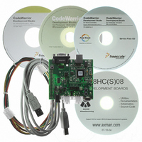
Manufacturer Part Number
DEMO9S08EL32
Description
BOARD DEMO FOR 9S08 EL MCU
Manufacturer
Freescale Semiconductor
Type
MCUr
Datasheets
1.DEMO9S08EL32.pdf
(356 pages)
2.DEMO9S08EL32.pdf
(14 pages)
3.DEMO9S08EL32.pdf
(2 pages)
Specifications of DEMO9S08EL32
Contents
Evaluation Board
Processor To Be Evaluated
MC9S08EL32
Data Bus Width
8 bit
Interface Type
RS-232, USB
Operating Supply Voltage
12 V
Silicon Manufacturer
Freescale
Core Architecture
HCS08
Core Sub-architecture
HCS08
Silicon Core Number
MC9S08
Silicon Family Name
S08EL
Rohs Compliant
Yes
For Use With/related Products
MC9S08EL32
Lead Free Status / RoHS Status
Lead free / RoHS Compliant


4.5
The MC9S08EL32 Series and MC9S08SL16 Series includes FLASH and EEPROM memory intended
primarily for program and data storage. In-circuit programming allows the operating program and data to
be loaded into FLASH and EEPROM, respectively, after final assembly of the application product. It is
possible to program the arrays through the single-wire background debug interface. Because no special
voltages are needed for erase and programming operations, in-application programming is also possible
through other software-controlled communication paths. For a more detailed discussion of in-circuit and
in-application programming, refer to the HCS08 Family Reference Manual, Volume I, Freescale
Semiconductor document order number HCS08RMv1/D.
4.5.1
Features of the FLASH and EEPROM memory include:
4.5.2
Before any program or erase command can be accepted, the FLASH and EEPROM clock divider register
(FCDIV) must be written to set the internal clock for the FLASH and EEPROM module to a frequency
(f
Register
reset initialization. FCDIV cannot be written if the access error flag, FACCERR in FSTAT, is set. The user
must ensure that FACCERR is not set before writing to the FCDIV register. One period of the resulting
clock (1/f
of these timing pulses is used by the command processor to complete a program or erase command.
Table 4-5
of FCLK (f
of cycles of FCLK and as an absolute time for the case where t
shown include overhead for the command state machine and enabling and disabling of program and erase
voltages.
Freescale Semiconductor
FCLK
•
•
•
•
•
•
•
) between 150 kHz and 200 kHz (see
Array size
— MC9S08EL32: 32,768 bytes of FLASH, 512 bytes of EEPROM
— MC9S08EL16: 16,384 bytes of FLASH, 512 bytes of EEPROM
— MC9S08SL16: 16,384 bytes of FLASH, 256 bytes of EEPROM
— MC9S08SL8: 8,192 bytes of FLASH, 256 bytes of EEPROM
Sector size: 512 bytes for FLASH, 8 bytes for EEPROM
Single power supply program and erase
Command interface for fast program and erase operation
Up to 100,000 program/erase cycles at typical voltage and temperature
Flexible block protection and vector redirection
Security feature for FLASH, EEPROM, and RAM
(FCDIV)”). This register can be written only once, so normally this write is performed during
FCLK
FLASH and EEPROM
shows program and erase times. The bus clock frequency and FCDIV determine the frequency
FCLK
Features
Program and Erase Times
) is used by the command processor to time program and erase pulses. An integer number
). The time for one cycle of FCLK is t
MC9S08EL32 Series and MC9S08SL16 Series Data Sheet, Rev. 3
Section 4.5.11.1, “FLASH and EEPROM Clock Divider
FCLK
= 1/f
FCLK
FCLK
= 5 μs. Program and erase times
. The times are shown as a number
Chapter 4 Memory
47
Related parts for DEMO9S08EL32
Image
Part Number
Description
Manufacturer
Datasheet
Request
R

Part Number:
Description:
Manufacturer:
Freescale Semiconductor, Inc
Datasheet:
Part Number:
Description:
Manufacturer:
Freescale Semiconductor, Inc
Datasheet:
Part Number:
Description:
Manufacturer:
Freescale Semiconductor, Inc
Datasheet:
Part Number:
Description:
Manufacturer:
Freescale Semiconductor, Inc
Datasheet:
Part Number:
Description:
Manufacturer:
Freescale Semiconductor, Inc
Datasheet:
Part Number:
Description:
Manufacturer:
Freescale Semiconductor, Inc
Datasheet:
Part Number:
Description:
Manufacturer:
Freescale Semiconductor, Inc
Datasheet:
Part Number:
Description:
Manufacturer:
Freescale Semiconductor, Inc
Datasheet:
Part Number:
Description:
Manufacturer:
Freescale Semiconductor, Inc
Datasheet:
Part Number:
Description:
Manufacturer:
Freescale Semiconductor, Inc
Datasheet:
Part Number:
Description:
Manufacturer:
Freescale Semiconductor, Inc
Datasheet:
Part Number:
Description:
Manufacturer:
Freescale Semiconductor, Inc
Datasheet:
Part Number:
Description:
Manufacturer:
Freescale Semiconductor, Inc
Datasheet:
Part Number:
Description:
Manufacturer:
Freescale Semiconductor, Inc
Datasheet:
Part Number:
Description:
Manufacturer:
Freescale Semiconductor, Inc
Datasheet: